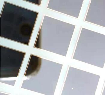
Core Product
Bare Silicon Photodiode Wafer (10×10 mm Die)
High linearity, common anode, ultra-low noise planar optical sensor chip.
Min. Order: 10 Pieces
A comprehensive technical evaluation on unencapsulated silicon photodetection substrates, junction physics, parasitic mitigation, and turnkey hybrid PCBA packaging.
In high-density optical instrumentation, medical diagnostic arrays, LiDAR front-ends, and quantum measurement setups, standard packaged photodiodes (such as TO-5, TO-18, or surface-mount SMD ceramics) introduce unacceptable optical and electrical compromises. Optical absorption from epoxy encapsulants, reflection at transmissive glass windows, parasitic pin capacitance (often exceeding 5 pF to 20 pF), and bulky physical envelopes drastically constrain the design window of modern optical platforms.
A bare silicon photodiode wafer presents a pure, planar semiconductor substrate where p-n, p-i-n, or avalanche junction arrays are directly fabricated into high-resistivity float-zone (FZ) or Czochralski (CZ) monocrystalline silicon. By acquiring photodetectors in unencapsulated bare wafer or diced die format, OEM design engineers can achieve direct Chip-on-Board (COB) or wire-bonded die integration immediately adjacent to ultra-low-noise transimpedance amplifiers (TIAs). This design paradigm collapses trace inductance, curtails thermal drift, eliminates window internal reflection losses, and achieves system bandwidths running in the hundreds of megahertz with sub-picowatt noise equivalent power (NEP).
When selecting bare silicon photodiode wafers, engineers encounter fundamental semiconductor trade-offs that dictate dynamic performance:
Shenzhen Mivo Electronics Co., Ltd. resolves the classic industry bottleneck between wafer foundries and PCBA assembly houses. While silicon fabs typically refuse to handle circuit assembly, and standard SMT factories refuse to handle unhoused bare dies, Mivo operates hybrid cleanroom mounting cells within our Shenzhen manufacturing campus. We dice wafers with micron-tolerance diamond saws, pick-and-place bare silicon photodiode dies directly onto high-frequency FR-4, ceramic, or aluminum core PCBs, execute gold/aluminum ultrasonic wire bonding, and deposit optical-grade silicone or hermetic conformal barriers—delivering ready-to-test optoelectronic PCBA modules under a single purchase contract.
Explore our core bare photodiode wafer options, alongside our custom turnkey PCB assembly, sensor probes, and companion optoelectronic components manufactured to client drawings.
High linearity, common anode, ultra-low noise planar optical sensor chip.
Min. Order: 10 Pieces
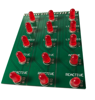
Built-in TIA transimpedance circuit for bare photodiode signal readout.
Min. Order: 5 Pieces
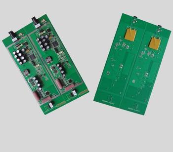
Impedance-controlled routing designed for multi-channel photodiode arrays.
Min. Order: 100 Pieces
Precision light-delivery probe matching silicon photodiode receiving stages.
Min. Order: 10 Pieces
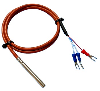
Monitors ambient thermal drift in calibrated laser & optical detection systems.
Min. Order: 10 Pieces
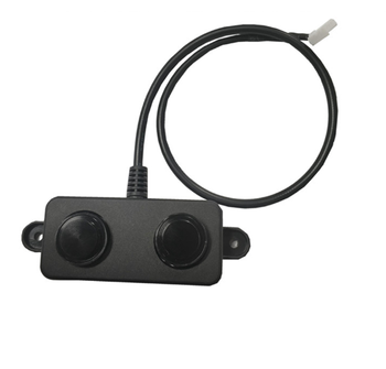
UART / PWM output sensor module with weather-sealed housing.
Min. Order: 10 Pieces
Require custom dice aspect ratios, segmented multi-cell quadrants, or wafer test mapping data?
Contact UsHow global purchasing managers and optoelectronics architects are adapting to AI-driven sensing demands, supply chain localization, and next-generation packaging architectures.
With artificial intelligence computing clusters demanding massive optical interconnect bandwidth, procurement trends are veering from discrete canned optical transceivers toward co-packaged optics. Bare silicon photodiode wafers diced into multi-channel linear arrays are directly bonded adjacent to silicon photonic modulators, slashing latency and interconnect power consumption by over 40%.
Historically, semiconductor wafer fabs demanded massive minimum batch commitments (MOQs of 25-wafer cassettes), locking out innovative startups and specialized medical developers. Modern procurement mandates maximum sourcing agility. Shenzhen Mivo Electronics provides engineering-grade low MOQ access—supporting prototype bare die orders starting from just 10 pieces with full wafer mapping.
As packaging and hybrid assembly costs increase, B2B procurement teams refuse to risk expensive substrates on untested silicon. The global trend mandates 100% automated wafer-level probe testing. Every die is mapped for reverse breakdown voltage ($V_{BR}$), dark current ($I_d$), and responsivity under calibrated reference light, providing digital wafer maps for pick-and-place automation.
Purchasing managers are actively eliminating multi-tiered supply friction. Sourcing bare silicon wafers from one continent, dicing in another, and flying dies to a third EMS provider leads to compound scrap rates and warranty finger-pointing. The modern trend unites wafer distribution, custom dicing, bonding, and turnkey PCBA fabrication under a single verified partner like Mivo Electronics.
Refer to our semiconductor engineering reference table before formulating your procurement request or technical datasheet submission.
| Parameter | Planar PN Junction Die | Planar PIN Photodiode Die | Segmented Quadrant / Multi-Array |
|---|---|---|---|
| Primary Mechanism | Shallow diffused p-n junction with zero/low bias operation | Intrinsic high-resistivity drift layer under reverse bias | Monolithic multi-anode wafer with isolation channels |
| Spectral Response | 320 nm – 1100 nm (Optimized for visible & UV) | 400 nm – 1100 nm (High NIR QE at 850–905 nm) | Custom tailored (Vis or NIR optimized) |
| Dark Current ($I_d$) | Extremely Low: 10 pA – 200 pA (Photovoltaic mode) | Moderate: 0.5 nA – 5 nA at $-5\text{V}$ reverse bias | Channel isolated: ≤ 1 nA per element |
| Response Time / BW | Microsecond scale (Best for precision DC measurement) | Nanosecond scale (> 100 MHz bandwidth capability) | Nanosecond to microsecond depending on die area |
| Junction Capacitance | High ($100\text{ pF} - 1000\text{ pF}$ depending on area) | Low ($5\text{ pF} - 50\text{ pF}$ under full depletion bias) | Individual pad capacitance strictly minimized |
| Typical Target Applications | Spectrophotometers, flame monitors, analytical chemistry | Laser rangefinders, LiDAR, optical data links, pulse sensors | Laser beam centering, angle tracking, confocal microscopy |
Combining verified semiconductor supply links, turnkey electronic assembly, and English-speaking engineering oversight in Shenzhen's hardware capital.
Shenzhen Mivo Electronics Co., Ltd. (established in 2016) bridges high-precision optical component sourcing with turnkey surface mount technology (SMT) and through-hole PCB assembly. For optical engineers, our dual capability resolves one of the toughest manufacturing dilemmas: semiconductor wafer manufacturers are unwilling to mount dies on circuit boards, while commercial PCB assembly plants refuse to touch bare semiconductor wafers.
At Mivo Electronics, our team of 51–100 manufacturing and quality professionals provides clean-environment die handling, precision wafer dicing, gold-wire bonding, and impedance-matched PCBA fabrication. Whether you require 10 pieces of diced silicon photodiode wafers for proof-of-concept laboratory calibration or volume production runs of thousands of integrated transimpedance PCBA modules, we maintain strict quality control.
Transparency is foundational to our client partnerships. Our manufacturing facility has passed rigid onsite verification by Alibaba.com and independent third-party audit companies. We maintain an average verified buyer rating of 4.7 out of 5 across more than 8 years of global exports, providing transparent documentation, verified test data, and seamless communication from design review to final delivery.
Established Year
Staff (51–100)
Facility Footprint
Export Track Record
Average Buyer Rating
Low MOQ Bare Die
Key technical answers addressing questions frequently raised by overseas optoelectronic buyers, test engineers, and supply chain managers.
Our engineering team in Shenzhen is ready to review your optical specifications, custom active area dimensions, and BOM files to deliver an optimized quote within 24 hours.
[email protected]