High-Layer Count Fabrication
Engineered multilayer stackups from 4 to 32 layers, supporting ultra-dense designs, heavy copper, and controlled dielectric cores.
- Up to 32 layers standard
- Aspect ratio up to 12:1
- High-Tg, Halogen-Free FR-4
Engineering high-density interconnect (HDI), controlled impedance layer stackups, and turn-key SMT assembly up to 32 layers for mission-critical hardware.
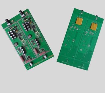
Rigid FR-4, HDI & High-Tg Multilayer Solutions
Advanced microvias, laser drilling, buried/blind via structures, and differential impedance matching calculated with Polar SI9000 accuracy.
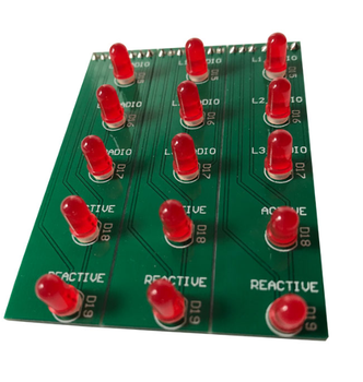
Turnkey Component Sourcing & SMT Placement
Direct access to Shenzhen's tier-1 supply networks, 0201 SMT precision, BGA X-ray inspection, and comprehensive functional testing under one roof.
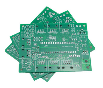
Comprehensive engineering insights addressing key inquiries raised by global procurement teams and hardware engineers when selecting a high-layer fabrication and turnkey PCBA partner.
When transitioning beyond 4 layers to 8, 12, or 24 layers, high-speed digital designs encounter severe electromagnetic interference (EMI), dielectric absorption, and signal cross-talk. At Shenzhen Mivo Electronics Co., Ltd., we mitigate these physical phenomena using rigorous pre-production impedance simulation via Polar SI9000, combined with low-loss, high-Tg copper-clad laminates such as Shengyi S1000-2M, ITEQ IT-180A, and Rogers hybrid dielectric packages.
Our etching chemistry maintains trace width tolerances of ±0.5 mil (±12.5 μm) on inner routing layers, guaranteeing differential impedance matching (±5% tolerance) on multi-gigabit interfaces like PCIe Gen 4/5, USB4, HDMI 2.1, and 10GbE copper channels. Dedicated ground planes isolate high-frequency differential pairs from noisy DC-DC switching rails, eliminating parasitic loop inductance.
Thermal stress during lead-free reflow (reaching peak temperatures of 260°C) often triggers catastrophic failures such as inner-layer delamination, barrel cracking in plated through-holes (PTH), and dielectric blistering. Shenzhen Mivo Electronics Co., Ltd. resolves this risk by optimizing the glass transition temperature (Tg ≥ 170°C) and curing cycles during hydraulic vacuum lamination.
By enforcing a low z-axis coefficient of thermal expansion (CTE ≤ 2.5% from 50°C to 260°C) and applying uniform resin flow prepregs (such as 1080 and 2116 weaves), we preserve interfacial copper adhesion. Furthermore, thermal via farms filled with non-conductive epoxy and capped with planar copper (VIPPO - Via-in-Pad Plated Over) dissipate concentrated heat away from fine-pitch BGAs into heavy ground planes.
Shenzhen Mivo Electronics Co., Ltd. consolidates multilayer bare-board manufacturing, components procurement, automated SMT, and testing to remove supply chain friction.
Engineered multilayer stackups from 4 to 32 layers, supporting ultra-dense designs, heavy copper, and controlled dielectric cores.
Microvia laser drilling, staggered and stacked blind/buried vias, and 1+N+1 to 3+N+3 sequential lamination for miniature products.
Direct integration into Shenzhen's authorized component distribution channels to guarantee 100% genuine passive and active silicon.
High-precision pick-and-place lines running 0201 passives, 0.35 mm pitch BGA assembly, automated optical inspection, and full functional validation.
Explore our most frequently ordered multilayer boards and turnkey sub-assemblies manufactured for global industrial, robotics, and communications clients.
Custom fabricated to your Gerber packages and stackup drawings.
4–32 layers · ENIG / Immersion Silver · Blind vias
Min. Order: 100 Pieces
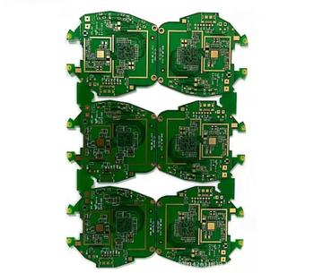
High-Tg FR-4 · Controlled impedance ±5%
Min. Order: 100 Pieces
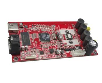
6–12 layer stackups · VIPPO process · Lead-free
Min. Order: 100 Pieces
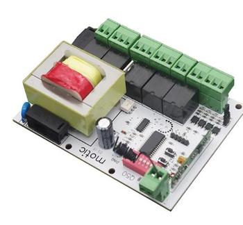
Signal integrity simulation · DFM optimization
Min. Order: 100 Pieces
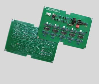
2–6 oz copper · High thermal conductivity
Min. Order: 100 Pieces
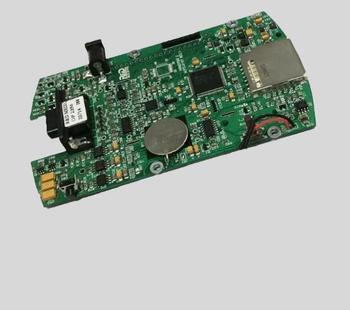
Automated wave soldering · Selective soldering
Min. Order: 100 Pieces
Fast-turn SMT mounting with full BOM trace purchasing.
SMT + BGA + DIP assembly · 100% AOI tested
Min. Order: 5 Pieces
Heavy copper trace layout · Thermal vias
Min. Order: 5 Pieces
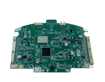
Complex multi-sensor inputs · Motor driving
Min. Order: 100 Pieces
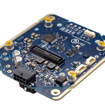
SWD/JTAG in-line testing · Automated testing
Min. Order: 5 Pieces
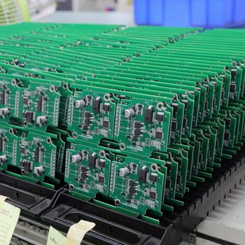
24–48 hour quickturn · 0201 parts capable
Min. Order: 5 Pieces
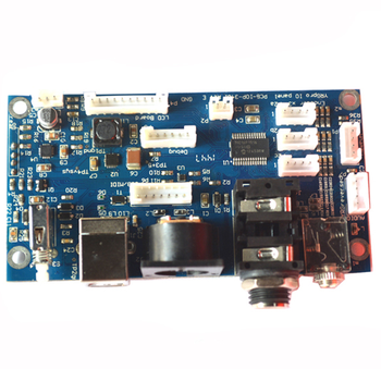
High-reliability thermal cycling · ISO standard
Min. Order: 5 Pieces
Custom measurement modules engineered for multilayer board integration.
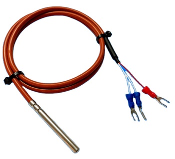
Silicone cable 1–5 m · waterproof, oil-proof
Min. Order: 10 Pieces
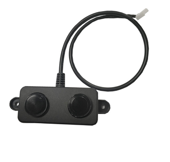
UART / PWM output
Min. Order: 10 Pieces
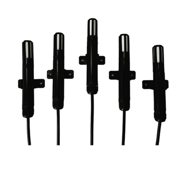
Waterproof, high-temperature air probe
Min. Order: 100 Pieces
M3 / M4 / M6 probe heads
Min. Order: 10 Pieces
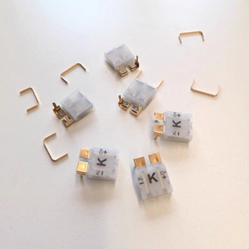
K / U type · vertical & right-angle
Min. Order: 100 Pieces
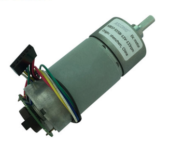
12 V · 16 PPR Hall encoder · high torque
Min. Order: 100 Pieces
How the market for multilayer printed circuit boards is shifting, and what hardware engineering teams should anticipate over the next five years.
Centrally stationed in Shenzhen's Yuanshan high-tech corridor, offering direct access to advanced PCB fabrication and Tier-1 electronic component supply lines.
Shenzhen Mivo Electronics Co., Ltd. is an onsite-verified manufacturer based in Shenzhen, Guangdong, China. We specialize in precision multilayer PCB manufacturing (from 4 to 32 layers), complex rigid-flex boards, aluminum core thermal boards, turnkey surface-mount PCBA, and electronic component procurement. Alongside board-level solutions, our manufacturing facilities assemble custom sensors (PT100 RTD probes, NTC thermistors, digital humidity modules), laser-cut SMT stencils, and industrial membrane switches.
Operating with a verified workforce of 51 to 100 professionals, we cater to hardware startups, OEM machinery manufacturers, and global engineering enterprises. We bridge the critical gap between fast prototype builds (starting from just 5 pieces) and scalable volume production. Our international trade team provides transparent, technical English-language project management, detailed DFM feedback within 12 hours, and comprehensive trace purchasing transparency.
Transparency is foundational to our partnerships. Our manufacturing facility has passed strict onsite checks by Alibaba.com and third-party auditing agencies. With over 8 years of continuous export operations and a 4.7 out of 5 buyer satisfaction rating, we guarantee full engineering accountability from initial Gerber review to global delivery.
Year Established
Employees (51–100)
Max Multilayer Count
Exporting Track Record
Buyer Rating Score
Min Prototype PCBA
Review the exact manufacturing capabilities and process tolerances enforced in our Shenzhen PCB fabrication facility.
| Process Parameter | Standard Capability | Advanced / High-Density Capability |
|---|---|---|
| Layer Count | 4 – 16 Layers | Up to 32 Layers (Custom up to 48L) |
| Base Laminates | Standard FR-4 (Tg 140–150°C) | High-Tg FR-4 (Tg ≥ 170°C), Rogers, Polyimide, Halogen-Free |
| Minimum Line Width / Spacing | 4 / 4 mil (0.10 mm / 0.10 mm) | 3 / 3 mil (0.075 mm / 0.075 mm) |
| Min. Mechanical Drill Hole | 0.20 mm (8 mil) | 0.15 mm (6 mil) |
| Laser Microvia Diameter | 0.10 mm (4 mil) | 0.075 mm (3 mil) |
| Aspect Ratio (PTH) | 8:1 | 12:1 |
| Impedance Control Tolerance | ±10% | ±5% (TDR Coupon Verified) |
| Surface Finishes | HASL Lead-Free, OSP | ENIG (Gold 1–3 u"), ENEPIG, Immersion Silver/Tin |
| Via Technologies | Tented / Plugged Vias | VIPPO (Via-in-Pad Plated Over), Blind & Buried Vias |
| Testing Standards | Flying Probe & AOI Testing | Bed of Nails, TDR Impedance, Microsection Cross-Sectioning |
Every order follows a documented, traceable fabrication cycle under strict ISO-compliant monitoring.
Comprehensive checks on inner annular rings, trace-to-copper clearances, via aspect ratios, and impedance modeling.
Direct imaging, precision inner layer copper etching, and automated optical inspection (AOI) before layer bonding.
High-pressure hot-press bonding of cores and prepregs under continuous vacuum to eliminate voids and inner blisters.
Mechanical drilling of through-holes and precision UV/CO2 laser ablation for blind/buried microvias with X-ray registration.
Electroless copper deposition followed by electrolytic acid plating, solder mask application, and ENIG/HASL chemical finishing.
100% flying probe / fixture electrical testing, TDR impedance coupon testing, followed by automated SMT placement.
Real-world engineering and purchasing answers addressing technical, cost, lead time, and assembly considerations.
Submit your Gerber files (RS-274X/ODB++) and BOM for a free, comprehensive DFM engineering review and instant quotation from our technical team.
[email protected]