Engineered Sensors, Thermal Coolers & Piezo Components
Precision-manufactured building blocks ready for seamless integration with custom membrane circuits, flexible printed electronics, and turnkey SMT control modules.
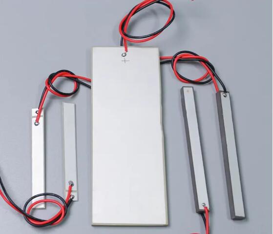
Piezo Ceramic Element PZT Long Strip Ultrasonic Experimental Transducer Wafer
Learn More →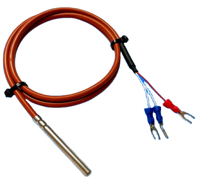
PT100 Temperature Sensor 5mm*50mm RTD Probe 3 Wire 1-5m Silicone Gel Coated
Learn More →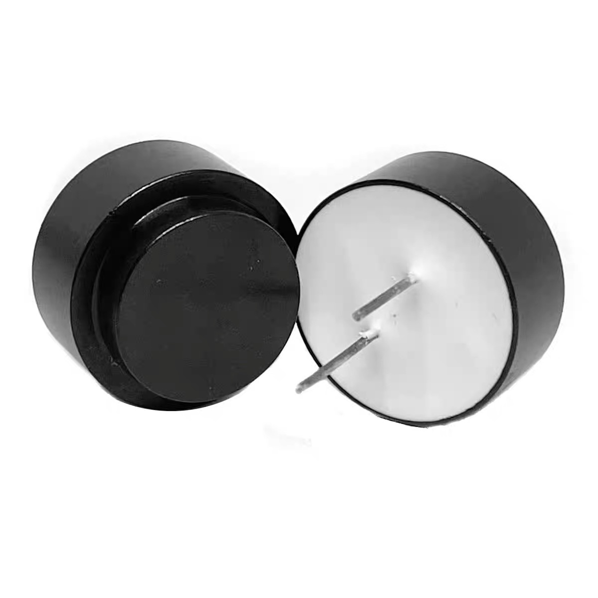
16mm Waterproof Ultrasonic Sensor Probe for Smart Home Car Distance Measurement
Learn More →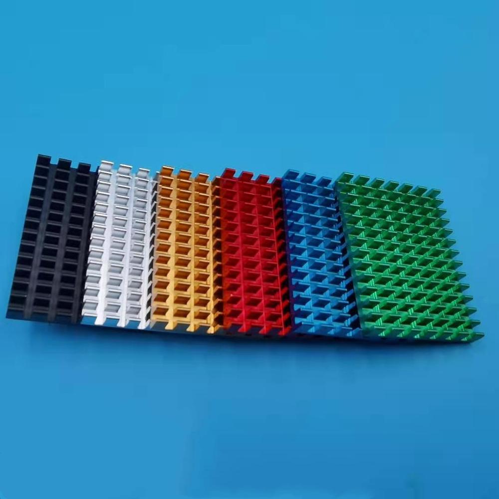
30*40*5MM Aluminum Profile Heat Sink Chip IC CPU Router Memory PCB Board Cooler
Learn More →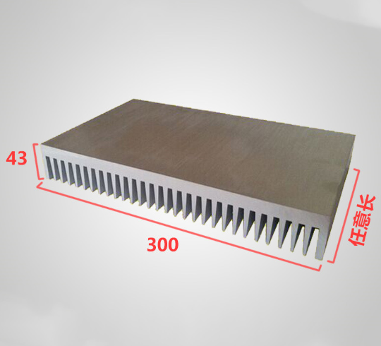
Cooling Plate 300*43*100/200/300mm Aluminum Radiator Width 300 High 43 Heat Sink
Learn More →
PZT Profiled-shape Piezoelectric Ceramic Semi-circular Sector Wave Guide Sensor
Learn More →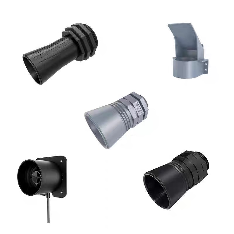
Ultrasonic Sensor Level Meter Down-well Ranging Water Level Measurement Module
Learn More →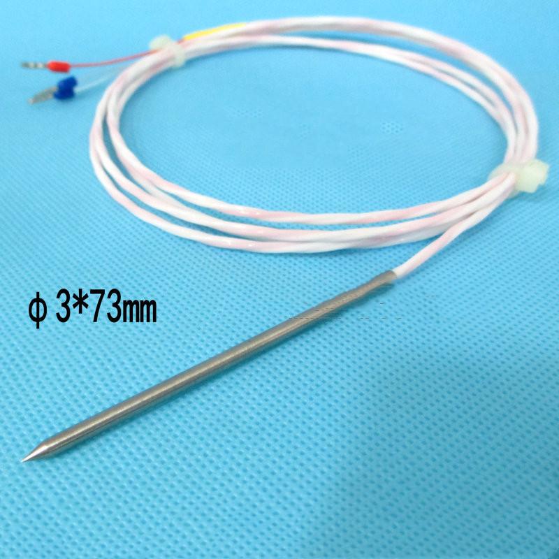
PT100B PT100A PT1000 Pointed End Thermal Resistance Platinum Thermistor Pierce Probe
Learn More →Membrane Circuit Engineering: Substrates, Conductive Traces & Layer Architecture
In modern industrial electronics, human-machine interfaces (HMI), and medical diagnostic instrumentation, the membrane circuit represents far more than a rudimentary electrical contact switch. It serves as a hermetically sealed, thin-profile, multi-layered flexible interconnect medium engineered to operate flawlessly in chemically aggressive, thermally erratic, and high-vibration operating environments. Manufactured by screen-printing conductive silver, carbon, or PEDOT:PSS polymeric inks onto dimensionally stabilized flexible substrates, membrane circuits bridge mechanical tactile feedback and solid-state logic controllers.
The foundational choice of substrate dictates flexural fatigue limits, thermal shrinkage thresholds, and moisture absorption characteristics. While Polyethylene Terephthalate (PET) remains the industry benchmark due to its superior mechanical shear strength and cost efficiency, engineering teams must specify heat-stabilized, biaxially oriented optical-grade PET (typically 125μm to 188μm) to mitigate trace registration drift during the thermal sintering cycles of conductive screen inks. For high-operating-temperature regimes ranging up to 150°C or applications mandating direct component soldering, Polyimide (PI) films or Polyethylene Naphthalate (PEN) substrates are deployed to maintain zero-delamination structural integrity.
Substrate Stabilization
Thermal pre-shrinking of optical-grade polyester films at 150°C for 30 minutes prevents multi-pass graphic registration errors and trace micro-cracking across consecutive thermal curing cycles.
Silver Trace Sintering
Precise thermal profile sintering controls conductive particle percolation, achieving sheet resistances under 0.015 Ω/sq/mil while maximizing cross-hatch ink adhesion.
Environmental Sealing
Continuous perimeter gas-gasket adhesive rings provide continuous IP65, IP67, or NEMA 4X ingress isolation, shielding sensitive contact pads from moisture and caustic industrial solvents.
A typical high-reliability membrane circuit stack consists of six distinct engineered layers: an anti-glare, chemical-resistant graphic overlay (Autotype Autotex polyester); an acrylic adhesive spacer layer (3M 467MP or 3M 468MP high-performance transfer tape); an upper circuit sheet carrying silver conductive traces; a vented center spacer defining the travel gap for tactile metal domes; a lower circuit sheet with matching contact interdigitated fingers; and a rear structural adhesive bonded to an aluminum backer plate or enclosure chassis. Vent channels are systematically engineered between dome chambers to normalize internal air pressure during rapid key actuations without admitting external ambient contaminants.
Membrane Circuitry vs. Rigid PCB vs. Flexible Printed Circuit (FPC)
Procurement directors and electronic hardware designers must constantly balance mechanical profile, assembly cost, chemical resistance, and tooling expense when architecting user-interface sub-assemblies. The table below delineates critical operational trade-offs across common flexible interconnect methodologies.
| Engineering Attribute | Printed Membrane Circuit (PET) | Etched Flexible PCB (PI FPC) | Rigid FR-4 Multilayer PCB |
|---|---|---|---|
| Primary Conductive Medium | Screen-printed Silver / Carbon Polymeric Paste | Subtractive Etched Copper Foil (ED or RA) | Electrodeposited Copper Laminate |
| Typical Circuit Thickness | 0.125 mm – 0.350 mm | 0.050 mm – 0.150 mm | 0.80 mm – 3.20 mm |
| Sheet Resistance | 10 to 50 mΩ/sq/mil (Ink-dependent) | < 0.5 mΩ/sq/mil (Ultra-low) | < 0.5 mΩ/sq/mil |
| Tactile Dome Integration | Direct integration without extra daughterboard | Requires secondary carrier or soldering | Requires discrete switches or snap domes |
| Tooling & Setup Investment | Low (Precision film phototools & stencils) | Moderate to High (Photolithography masks) | Moderate (Drill & SMT tool sets) |
| Moisture / Solvent Immunity | IP67/NEMA 4X monolithic front seal | Requires conformal coating / potted seal | Requires mechanical O-rings & gasket seals |
| SMT Component Soldering | Low-temp conductive epoxy bonding (SMT LEDs) | Standard lead-free reflow (SAC305) | Standard lead-free reflow & wave soldering |
While polyimide-based FPCs excel in carrying higher drive currents and accommodating micro-pitch BGA packages, printed silver membrane circuits dominate cost-sensitive, large-surface user interfaces. The elimination of expensive copper etching chemistry, coupled with the ability to integrate keypads, LED backlighting, and environmental sealing into a monolithic thin-film sandwich, renders printed membrane circuits the undisputed benchmark for industrial machinery, commercial dishwashers, vehicle instrumentation panels, and medical infusion systems.
Overcoming Silver Migration: Metallurgy & Dielectric Encapsulation
The single greatest operational hazard threatening silver-printed flexible electronics is electrochemical migration (dendritic growth). Under the simultaneous influence of electrical bias (voltage potential), elevated ambient humidity, and ionic contaminants, silver ions (Ag+) dissolve from anode traces and migrate across the dielectric substrate to form branching microscopic metallic dendrites at the cathode. Left unaddressed, these dendrites eventually cause catastrophic high-resistance shorts and circuit malfunctions.
At Shenzhen Mivo Electronics Co., Ltd., our engineering methodology eliminates silver migration risks through three redundant design rules:
Carbon Paste Overprinting
Every exposed silver trace pad, contact finger, and connector interface is completely enveloped with a polymer thick-film carbon ink overprint. Carbon acts as an electrochemical buffer that physically halts silver atom dissolution even under moisture condensation.
UV-Curable Dielectric Bridges
Where trace crossing or dense multi-line routing is required, dual-pass cross-linked UV dielectric insulating inks are deposited. The cured dielectric film exhibits breakdown voltages exceeding 1,500 V/mil and complete non-porosity.
Creepage & Pitch Optimization
Our DFM review mandates minimum trace-to-trace spacing tolerances based on operating voltages: a minimum of 0.50 mm pitch for signals ≤ 12V DC, scaling up to 1.00 mm for 24V DC industrial bus traces to minimize electric field intensity.
Coupled with our automated optoelectronic AOI inspection and environmental climate chamber validation (-40°C to +85°C at 95% RH for 500 hours), our membrane circuit assemblies guarantee continuous mean time between failures (MTBF) exceeding 5,000,000 mechanical actuations.
Future Procurement Trends: Where Printed Flexible Electronics Is Heading
Global supply chain directors and hardware procurement teams are redefining their sourcing matrices to navigate raw material volatility, environmental regulatory compliance, and rapid technological convergence. Based on our 8-year operational tenure on international manufacturing platforms and direct technical interactions with overseas procurement directors, we identify four critical trends transforming the membrane circuit supply chain:
In-Mold Electronics (IME)
Transition from flat 2D membrane panels to structural 3D thermoformed parts. Conductive traces and touch sensors are printed directly on the substrate prior to high-pressure injection molding.
Decoupled Hybrid PCBA
Combining rigid FR-4 control boards with flexible printed membrane tails and zero-insertion-force (ZIF) crimp connectors to simplify modular field repair and lower overall bill of materials (BOM).
Green Chemistries
Adoption of bio-derived PET films and low-VOC conductive water-based inks to meet strict EU RoHS 3.0, REACH, and California Proposition 65 directives without sacrificing adhesive shear performance.
Sensorized Interfaces
Integrating piezoresistive pressure sensors, force-sensing resistors (FSRs), and capacitive slider channels directly onto the membrane substrate for sleek button-free modern equipment interfaces.
To preserve procurement margins against precious metal commodity fluctuations (specifically industrial silver pricing), savvy buyers are transitioning low-current ground planes and static shielding layers from pure silver to high-conductivity silver-coated copper blends or specialized conductive carbon graphite pastes, driving down unit procurement costs by 15% to 28% without altering contact impedance.
Enterprise Strengths: Shenzhen Mivo Electronics Co., Ltd.
Headquartered in the global electronics nexus of Shenzhen, Guangdong (Yuanshan Street), Shenzhen Mivo Electronics Co., Ltd. has served international OEMs, medical device innovators, and industrial equipment builders since 2016. Operating within the world's most dense component sourcing and PCB assembly ecosystem, we offer buyers unmatched agility, compressed turnaround windows, and rigorous quality governance.
Unlike conventional middleman brokers, our premises have passed rigorous onsite physical verification by Alibaba.com staff and third-party inspection agencies. We maintain an audited 4.7 out of 5 buyer rating across eight continuous years of global trade history. Our vertically integrated operations span bare board fabrication, flexible printed circuits, SMT solder paste stencils, membrane switch panels, and turnkey PCBA assembly starting from minimum orders as low as 5 pieces for prototyping to volume runs exceeding 100,000 units.
Engineering DFM Scrutiny
Our engineering staff reviews your RS-274X Gerber files, BOM component part numbers, and centroid pick-and-place files to resolve trace impedance and footprint discrepancies prior to tooling release.
Turnkey Sourcing Ecosystem
Direct integration into the Huaqiangbei / Shenzhen electronic component distribution corridors ensures authentic ICs, passives, and mechanical hardware at tier-one volume pricing with zero grey-market risks.
100% Functional Test Matrix
Every membrane circuit and assembled PCBA undergoes full electrical continuity screening, contact resistance verification (< 100 Ω), insulation testing (> 100 MΩ at 100V DC), and tactile switch actuation cycle checks.
Beyond membrane circuitry, our manufacturing catalog encompasses precision PT100/PT1000 RTD temperature sensor probes, high-frequency ultrasonic transducers, extruded aluminum heatsink cooling profiles, and planetary gearmotors. This comprehensive electro-mechanical portfolio empowers our clients to consolidate complex multi-vendor bills of materials into a single accountable, verified manufacturing partner.
Membrane Circuit Procurement & Manufacturing FAQ
Comprehensive engineering clarifications addressing the most common technical inquiries submitted by international purchasing managers and system integration engineers.
What engineering files and documentation are required to initiate custom membrane circuit manufacturing?
What is the typical mechanical lifespan of stainless steel tactile snap domes versus non-tactile polydomes?
Can surface-mount LEDs and active components be mounted directly onto a flexible membrane circuit?
What is the standard tooling lead time and Minimum Order Quantity (MOQ) for custom membrane switches?
How does your factory ensure graphic overlay color matching and chemical resistance?
How does Mivo Electronics handle obsolete electronic components in the PCBA bill of materials?
Request an Engineering Quote for Your Custom Membrane Circuit
Send your drawings, Gerber layers, and BOM files to our Shenzhen technical engineering office. We provide complimentary DFM reviews, prototype pricing, and lead time estimates within 24 business hours.