Complementary Sensor Probes, Assemblies & Control Hardware
Single-sided flexible PCBs serve as the foundational interconnect backbone across industrial instrumentation, power electronics, and high-reliability temperature monitoring devices. Browse our proven modules and precision-assembled hardware.
Single-Sided Flexible PCB: Fundamentals & Layer Stackup Topology
A single-sided flexible printed circuit (1-Layer FPC) consists of a single conductive copper layer laminated onto a flexible dielectric film, encapsulated by an insulating coverlayer. When designed correctly, single-sided flex circuits deliver the lowest profile, highest dynamic flex life, and maximum volumetric efficiency in modern electronics design.
Substrate Selection: PI vs. PET
Polyimide (PI) remains the undisputed gold standard for high-reliability solderable FPCs, operating continuously from -200°C to +260°C. Polyester (PET) offers an economical substrate for low-temperature membrane switches and passive wiring harnesses where reflow soldering is avoided.
- PI Thickness Range: 12.5µm (0.5 mil) to 50µm (2.0 mil)
- PET Glass Transition (Tg): ~75°C to 110°C
- Dielectric Breakdown: > 150 kV/mm (Kapton® grade)
Copper Foil: RA vs. ED Microstructure
Rolled Annealed (RA) copper features elongated, horizontally oriented grain structures capable of enduring millions of continuous dynamic bend cycles without mechanical fracture. Electro-Deposited (ED) copper offers vertical grain columns, suited for static bend-to-install geometries.
- RA Fatigue Cycle Limit: > 10,000,000 cycles (R=10t)
- ED Application: Static installation, 3D form-factor routing
- Standard Weights: 1/3 oz (12µm), 1/2 oz (18µm), 1 oz (35µm)
Encapsulation & Stiffener Bonding
Flexible coverlayers consisting of polyimide film backed with thermo-curable modified acrylic or epoxy adhesives seal etched copper traces from oxidation, flux contamination, and physical abrasion. Localized FR-4, PI, or stainless steel stiffeners ensure coplanar ZIF connector seating.
- Coverlay Thickness: 12.5µm/15µm, 25µm/25µm (Film/Adhesive)
- Stiffener Variety: FR4 (0.2–1.6mm), SUS304 (0.1–0.3mm), PI
- Bonding Adhesives: Thermosetting resin / 3M VHB PSA
| Material / Engineering Parameter | Adhesiveless Polyimide (2-Layer FCCL) | Adhesive-Based Polyimide (3-Layer FCCL) | Polyester Base (PET) |
|---|---|---|---|
| Thermal Endurance & Reflow | Lead-free solder compatible (>288°C, 30s) | Standard reflow (240°C–260°C maximum) | Low-temp silver paste / crimping only (<105°C) |
| Dynamic Flex Fatigue Life | Superior (Zero adhesive shear fatigue) | Good (Adhesive layer cushions micro-stress) | Moderate to Poor (Subject to micro-cracking) |
| Dielectric Constant (Dk @ 1 GHz) | 3.2 – 3.4 (Predictable high-speed RF) | 3.5 – 3.7 (Influenced by adhesive resin) | 3.0 – 3.2 |
| Minimum Dynamic Bend Radius | 6× to 10× Total Stack Thickness | 10× to 15× Total Stack Thickness | 20× to 30× Total Stack Thickness |
| Peel Strength (N/mm, As Received) | ≥ 0.9 N/mm (Cast/Thermal compression) | ≥ 1.2 N/mm (Acrylic bond chemistry) | ≥ 0.7 N/mm |
Future Procurement & Sourcing Trends in Flexible Circuitry
Procuring single-sided flexible printed circuits has shifted from simple component-level commoditization to integrated electro-mechanical sub-assembly sourcing. Hardware engineers and procurement leads must navigate the following macro shifts to mitigate supply risk and maintain target bill-of-materials (BOM) margins.
1. Roll-to-Roll (R2R) Continuous Processing
OEM volume purchasers are transitioning from traditional sheet-fed (panel-by-panel) batch processing to automated continuous web Roll-to-Roll (R2R) manufacturing lines. R2R wet processing and laser direct imaging (LDI) reduce handling defects, eliminate human panel-transfer scratches, and lower total unit cost by 18% to 35% on runs exceeding 50,000 meters.
2. EV Battery Cell Contacting Systems (CCS)
Automotive battery management systems (BMS) are replacing bulky traditional round-wire harnesses with single-sided, ultra-long (up to 1,500mm) flexible printed circuits. Integrated with surface-mount NTC thermistors, nickel battery tabs, and fuse links, single-sided FPCs minimize pack z-height while automating robotic pick-and-place pack integration.
3. Halogen-Free & Sustainable Green Substrates
Stricter RoHS 3, REACH, and UL94 V-0 flammability mandates have accelerated procurement of phosphorus-based halogen-free flame-retardant coverlayers. Furthermore, bio-based polyimide resins and closed-loop copper etchant reclamation systems are becoming core selection criteria for European and North American tier-1 enterprises.
Technological Trajectories Shaping Single-Sided Flex PCBs
As consumer wearables, medical endoscopy instruments, and defense guidance electronics compress volumetric packaging constraints, single-sided flex circuit fabrication technology is evolving toward extreme miniaturization.
Laser Direct Imaging & UV Laser Routing
Eliminating hard-tooling mechanical dies, high-precision UV/Picosecond laser systems ablate coverlayer openings down to 50µm diameters without causing thermal charring or heat-affected zone (HAZ) delamination. Concurrently, Laser Direct Imaging (LDI) enables fine-line trace geometries down to 35µm line/space (1.4 mil) on ultra-thin 1/3 oz copper foils.
Surface Finishes: Electroless Nickel Immersion Gold
While Hot Air Solder Leveling (HASL) induces excessive thermal shock and uneven coplanarity on thin flexible films, chemical finishes such as ENIG (Electroless Nickel Immersion Gold), Immersion Silver, and Organic Solderability Preservatives (OSP) dominate. ENIG provides an atomically flat contact pad ideal for fine-pitch SMT assembly, ZIF connectors, and gold wire bonding.
Embedded Shielding & Silver Paste Cross-Hatching
To combat electromagnetic interference (EMI) without compromising mechanical flexibility, manufacturers print conductive silver pastes or laminate specialized ultra-thin metallic shielding films (e.g., Tatsuta, Toyo) directly over the coverlayer. Cross-hatch copper ground structures preserve bending compliance while preventing impedance discontinuities.
Onsite-Verified Shenzhen Engineering Authority
Shenzhen Mivo Electronics Co., Ltd. operates at the center of the world's most agile electronics manufacturing cluster in Shenzhen, Guangdong. Backed by an onsite-verified production facility and a specialized technical workforce of 51 to 100 personnel, we bridge the gap between initial low-volume rapid prototyping and full-scale OEM/ODM production runs.
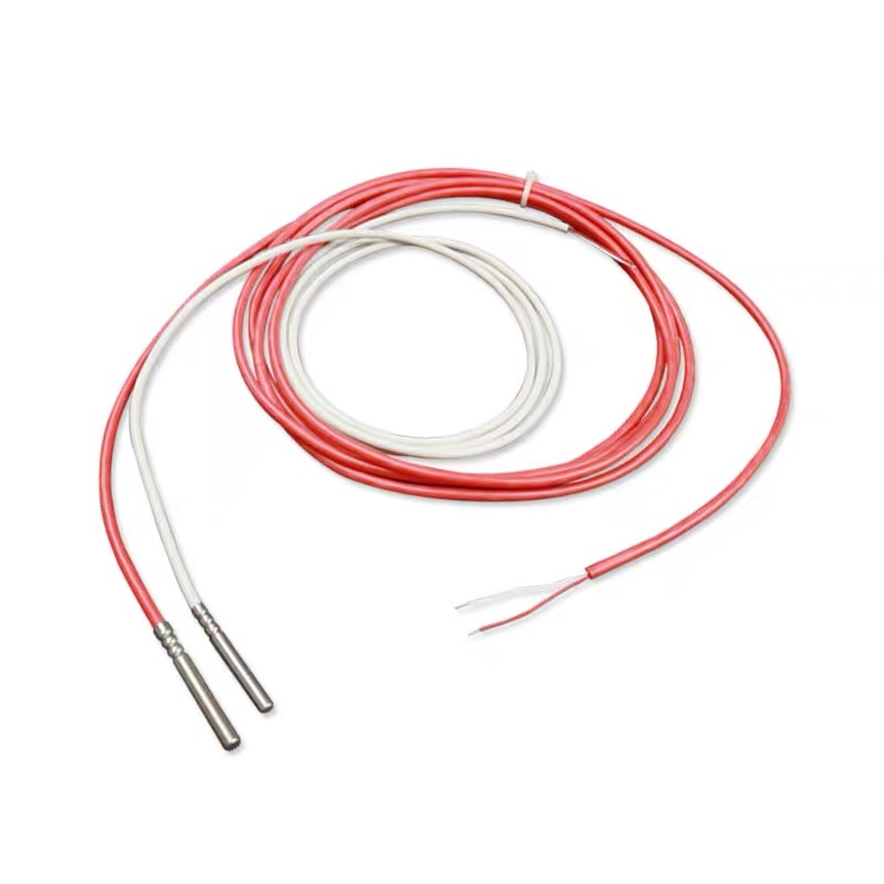
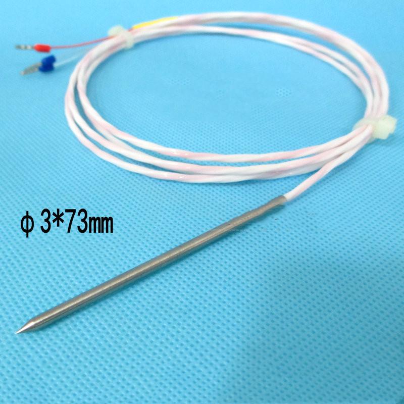
Our turnkey capabilities extend beyond bare single-sided flexible PCB fabrication: we source precision active and passive BOM components directly from certified tier-1 authorized distributors, manufacture custom RTD temperature sensors (PT100/PT1000/NTC), produce laser-cut SMT stencils, and execute high-yield flexible SMT assembly on rigid magnetic backing carriers.
With an 8-year global export track record and a 4.7 out of 5 verified buyer satisfaction rating, our DFM (Design for Manufacturability) engineering team inspects every Gerber (RS-274X) package, mechanical drawing, and pick-and-place centroid coordinate before copper etching begins.
Audited Production Metrics
- Legal Corporate EntityShenzhen Mivo Electronics Co., Ltd.
- Production Facility BaseYuanshan Street, Shenzhen, China
- Factory Audit VerificationAlibaba Onsite Checked & Verified
- Active Workforce Scale51 – 100 Engineering & SMT Staff
- Production Capacity ClassSingle-Sided FPC, Multilayer PCB, PCBA
- Assembly Prototype MinimumStarts from 5 Pieces
- Global Quality Evaluation4.7 / 5.0 Star Rating (8+ Years)
Frequently Asked Questions: Single-Sided Flexible PCB
Clear, direct engineering answers addressing high-intent manufacturing, design, and procurement questions raised by hardware development teams.
What constitutes the primary stackup of a single-sided flexible PCB?
How do I calculate the minimum bend radius for a single-sided flex circuit?
• Static Applications: The minimum bend radius should be at least 6× to 10× the total overall stackup thickness ($R \ge 10 \times T$).
• Dynamic Flexing Applications: The minimum bend radius must be maintained at a minimum of 20× to 40× the total overall thickness ($R \ge 20 \times T$). To optimize dynamic life, traces must be positioned along the neutral mechanical bending axis, conductor corners must be radiused rather than angled at 90°, and rolled annealed (RA) copper must always be specified.
Why should an engineer choose a coverlayer over standard Liquid Photoimageable (LPI) solder mask?
What are the advantages of adhesiveless flexible copper clad laminate (FCCL)?
How are surface-mount components (SMT) assembled onto thin single-sided FPCs?
What files and documentation are required to quote and manufacture a custom FPC?
What quality inspection standards are applied to single-sided flexible circuits?
Launch Your Custom Single-Sided Flexible PCB Project
Connect directly with our senior application engineers in Shenzhen. From single-piece functional prototyping to multi-million-unit mass production runs, we provide detailed DFM analysis and competitive tier-1 factory pricing.