Engineered HDI Hardware, Modules & Precision Components
From advanced micro-via circuit infrastructure to specialized electro-mechanical thermal components, explore our export-certified hardware lineup for Adelaide OEMs and hardware developers.
Localized HDI PCB Applications Across South Australia
Adelaide has established itself as Australia's cradle of space commercialization, modern defense modernization, and medical robotics. Our High-Density Interconnect (HDI) solutions solve critical volumetric and signal integrity challenges across regional hubs.
Lot Fourteen Defense & Aerospace
Adelaide's premier innovation precinct Lot Fourteen and the Osborne Naval Shipyard demand micro-pitch BGA packaging, Any-Layer HDI (ELIC), and low-loss substrates. Our boards operate seamlessly inside radar telemetry, tactical edge-computing devices, and low-earth orbit (LEO) nanosatellite constellations.
Tonsley Innovation District MedTech
From portable diagnostic ultrasonography to implantable biomedical monitors designed around Tonsley, circuit footprints require strict biocompatibility and high-density micro-via arrays. We provide blind and buried microvias down to 0.075 mm, allowing ultra-dense integration without cross-talk.
AgTech & Mining Industrial Telemetry
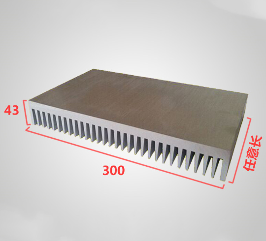
Operating in the harsh South Australian Outback requires electronics that endure extreme thermal variations and severe vibration. Our heavy copper HDI configurations, coupled with extruded aluminum thermal plates and potting-ready seals, deliver continuous field operations in remote telemetry hubs.
Adelaide High-Tech Manufacturing Trends & Engineering Demands
A comprehensive examination of why South Australian procurement teams and hardware engineering groups are migrating toward overseas OEM/ODM partnerships for HDI board fabrication.
| HDI Engineering Parameter | Standard Commercial Grade | Adelaide High-Rel Defense / MedTech Spec | Mivo Electronics Capabilities |
|---|---|---|---|
| Layer Count & HDI Architecture | 4 - 8 Layers (1+N+1) | 10 - 24+ Layers (Any-Layer / ELIC 3+N+3) | Up to 32 Layers, ELIC Any-Layer Micro-via |
| Laser Micro-Via Drill Diameter | 0.12 - 0.15 mm | 0.075 - 0.10 mm (Stacked & Staggered) | Down to 0.065 mm UV Laser Micro-drilling |
| Line Width / Space (Trace/Space) | 75 / 75 µm (3 / 3 mil) | 40 / 40 µm (1.6 / 1.6 mil) | Sub-35 µm Ultra-Fine Line Routing |
| Base Materials & Laminates | Standard FR-4 (Tg 140°C) | High Tg (180°C+), Megtron 6, Rogers RO4350B | Isola, Rogers, Panasonic Megtron, Taconic |
| Microvia Filling & Surface Finish | Non-conductive ink, HASL | Copper Paste Filled (VIPPO), ENIG, ENEPIG | Full Copper Via Fill (VIPPO), Electroless Nickel Immersion Gold |
Transition to Miniaturized Form Factors in South Australia
The convergence of AI at the edge, advanced unmanned aerial systems (UAS), and marine sonar arrays developed along the Port Adelaide industrial belt has rendered conventional through-hole multi-layer boards obsolete. High-speed signal paths demand short trace lengths to minimize parasitic capacitance and skin effect losses at multi-gigahertz frequencies.
By implementing Via-in-Pad Plated Over (VIPPO) structures alongside ultra-fine line widths down to 35 microns, Adelaide hardware designers can place high-pin-count 0.4mm pitch BGAs directly over blind microvias, reducing PCB layer count and assembly footprint by up to 45%.
Overcoming Australian Supply Chain Bottlenecks
While rapid local prototyping exists in Australia, volume scale-up often hits bottlenecks regarding specialized base laminates, specialized SMT stencils, and multi-axis automated optical and X-ray inspection (AXI). Local Adelaide procurement specialists frequently face lead times exceeding 8 to 12 weeks for complex Any-Layer builds.
Shenzhen Mivo Electronics bridges this gap by marrying Shenzhen's unmatched electronic supply ecosystem with strict Western engineering quality standards. We maintain direct stock of specialized RF high-frequency laminates and maintain dedicated high-speed SMT lines that transition projects from prototype to production seamlessly.
Enterprise Strengths: Shenzhen Powerhouse with Direct Adelaide Exporting
Backed by 8 years of onsite-verified exporting history, transparent procurement methodologies, and comprehensive turnkey assembly workflows.
Onsite-Verified Manufacturing
Premises inspected and legally confirmed by independent third-party assessors and Alibaba global enterprise compliance checks.
Full BOM Turnkey Traceability
Every active and passive component is sourced directly from certified franchise distributors, with written sign-off required for any lifecycle alternatives.
Low MOQ Prototyping (From 5 Pcs)
We eliminate high barrier costs for South Australian startups and university incubators by manufacturing pilot PCBA batches starting at just 5 pieces.
Direct Adelaide Air Express
Daily international freight departures guarantee door-to-door delivery across Adelaide CBD, Edinburgh Parks, and Lonsdale in as little as 3-5 business days.
Frequently Asked Questions for Adelaide Hardware Buyers
Clear, direct answers regarding customs, logistics, compliance certifications, and file preparation for importing into South Australia.
How are customs duties and GST handled when importing PCBs into Adelaide?
What engineering documentation is required to initiate an HDI quotation?
Do you support IPC Class 3 standards for medical and defense applications?
How does your turnkey component procurement manage global semiconductor shortages?
What is the standard turnaround lead time for prototypes delivered to South Australia?
Accelerate Your Adelaide Hardware Production
Whether you require 5 high-density prototype boards for validation or high-volume repeat runs, our engineering team is ready to analyze your Gerbers, optimize your BOM, and provide end-to-end manufacturing support.