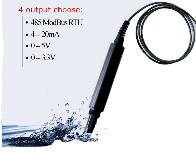
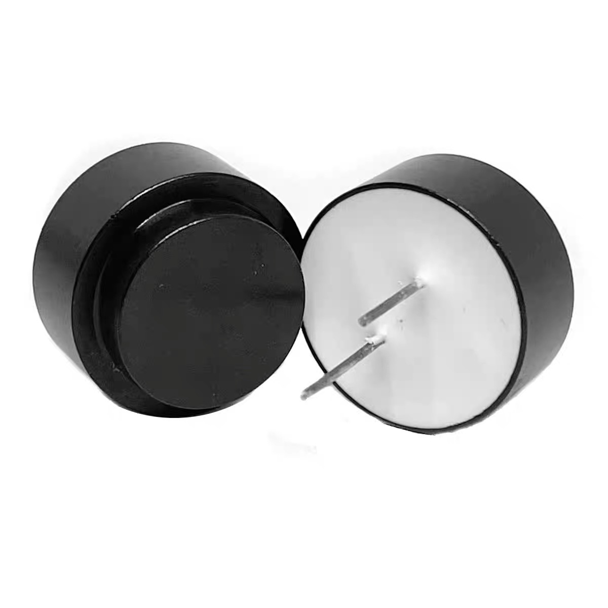
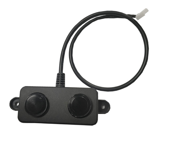
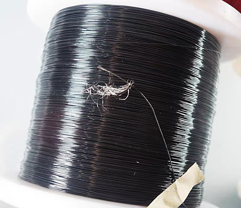
Featured Sensor Probes, Modules & Precision Assemblies
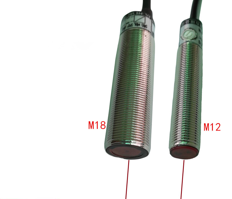
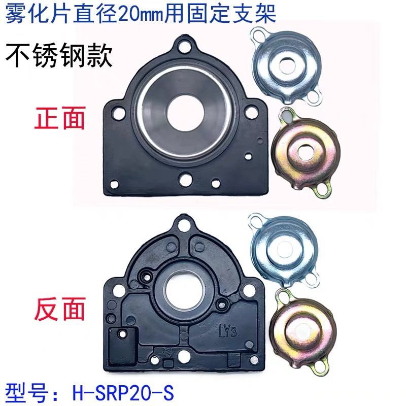
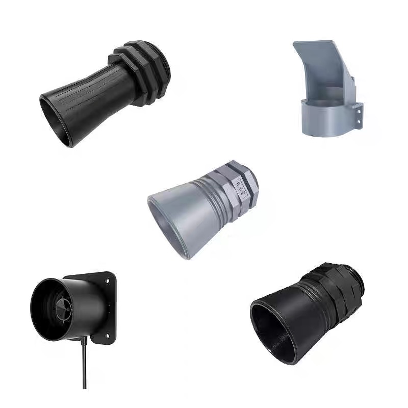
Engineered to integrate seamlessly with double-sided flexible printed circuits, multi-channel wiring harnesses, and dense industrial transducer arrays. Explore standard catalog specifications available for custom prototype runs.
The Engineering Fundamentals of Double Sided Flexible Printed Circuits (FPC)
Double-sided flexible printed circuits (FPCs) represent the backbone of contemporary high-density interconnect (HDI) hardware design, enabling three-dimensional volumetric packing, continuous dynamic flexing, and weight reduction that rigid FR-4 substrates cannot achieve. Unlike single-sided circuits that route current along a solitary conductive plane, double-sided FPCs incorporate conductive copper foil patterns laminated across both sides of an insulating base film—predominantly polyimide (PI). Signal and power connections between the top and bottom conductive layers are established using precision Plated Through-Holes (PTH) or ultraviolet/CO2 laser-drilled microvias.
In critical medical robotics, automotive sensor harnesses, folded smart-device displays, and aerospace avionics, double-sided flexible PCBs eliminate discrete point-to-point wire harnesses, mitigating mechanical human error during assembly and ensuring continuous impedance control across signal channels. However, the engineering complexity of manufacturing double-sided FPCs is substantially higher than rigid counterparts: the physical anisotropy of polyimide films, thermal expansion differentials during lamination, and moisture absorption kinetics mandate strict process controls across cleanrooms, etching bays, and surface metallization lines.
Cross-Sectional Anatomical Stackup of a Double-Sided Flexible Board
Designing a high-yield double-sided FPC requires meticulous balancing of the neutral bending axis to prevent inner-layer copper strain during dynamic operation. Below is the typical IPC-compliant symmetrical stackup utilized by Tier-1 aerospace and medical fabricators:
| Layer Index | Component Element | Standard Thickness (Metric/Imperial) | Material Specification | Functional Contribution |
|---|---|---|---|---|
| Layer 1 (Top) | Top Coverlay / Flexible Solder Mask | 12.5 µm PI + 15 µm Adhesive (1.1 mil total) | Kapton Polyimide / Modified Epoxy | Dielectric barrier, chemical resistance, physical abrasion shield |
| Layer 2 | Top Conductive Trace Foil | 18 µm (1/2 oz) or 35 µm (1 oz) | Rolled Annealed (RA) Copper | High-elongation electrical routing for dynamic flex zones |
| Layer 3 (Core) | Core Dielectric Base Film | 25 µm (1.0 mil) or 50 µm (2.0 mil) | Adhesiveless Polyimide Film | Substrate mechanical integrity, electrical dielectric separation |
| Layer 4 | Bottom Conductive Trace Foil | 18 µm (1/2 oz) or 35 µm (1 oz) | Rolled Annealed (RA) Copper | Secondary signal routing, controlled ground reference planes |
| Layer 5 (Bottom) | Bottom Coverlay / Protective Film | 12.5 µm PI + 15 µm Adhesive (1.1 mil total) | Kapton Polyimide / Modified Epoxy | Hermetic environmental seal and neutral axis balance |
Rolled Annealed (RA) copper foil is explicitly chosen over Electro-Deposited (ED) copper in double-sided dynamic applications because its horizontally oriented grain lattice structure tolerates repetitive compression and tension without generating micro-fissures. Conversely, ED copper is reserved for static "flex-to-install" applications where trace routing demands ultra-fine pitches below 50 µm (2 mil) line and space.
Top 10 Double Sided Flexible PCB Manufacturers & Exporters Worldwide
A comparative evaluation assessing technical capabilities, cleanroom automation, minimum trace resolution, prototype agility, and international export supply chain efficiency.
| Manufacturer / Exporter | Primary HQ & Facilities | Min. Trace / Space (L/S) | Specialization Focus | Prototyping & Turnaround Agility | Export Accreditations |
|---|---|---|---|---|---|
| Shenzhen Mivo Electronics Co., Ltd. | Shenzhen, Guangdong, China | 0.05 mm / 0.05 mm (2 / 2 mil) | Turnkey PCBA, Sensors, Custom Double-Sided FPC, Low-to-Medium Volume | Rapid Turn (From 5 pcs), Onsite Verified, Agile Engineering DFM | ISO9001, RoHS, REACH, Alibaba Verified |
| Nippon Mektron (NOK Group) | Tokyo, Japan / Global | 0.025 mm / 0.025 mm (1 / 1 mil) | Ultra-high volume smartphone displays, automotive ADAS | Geared toward automotive mass production contracts | IATF 16949, ISO 14001, ISO 9001 |
| Zhen Ding Technology Holding | Taoyuan, Taiwan / Shenzhen | 0.030 mm / 0.030 mm | Consumer electronics modules, flexible HDI, semiconductor packaging | Massive mega-scale production lines; high prototype MOQs | ISO 9001, IATF 16949, QC 080000 |
| Sumitomo Electric Interconnect | Osaka, Japan | 0.035 mm / 0.035 mm | Fluoropolymer FPCs, high-speed telecommunications, EV battery harnesses | Standard corporate lead times for automotive OEMs | IATF 16949, ISO 13485, AS9100 |
| MFLEX (Multi-Fineline Electronix) | California, USA / Suzhou, China | 0.035 mm / 0.035 mm | Medical instruments, industrial automation, defense flex solutions | Fast US-based NPI design with high-volume China scale | ISO 13485, AS9100D, ITAR Registered |
| Fujikura Ltd. | Tokyo, Japan / Thailand | 0.030 mm / 0.030 mm | Optical transceiver flex, disk drive assemblies, high-durability FPC | Long-cycle engineering validation for enterprise equipment | ISO 9001, IATF 16949, ISO 14001 |
| Interflex Co., Ltd. | Ansan, South Korea | 0.030 mm / 0.030 mm | Rigid-Flex, OLED touch display interconnects, camera modules | High-throughput consumer electronics delivery cycles | ISO 9001, IATF 16949 |
| BH Co., Ltd. | Incheon, South Korea / Vietnam | 0.035 mm / 0.035 mm | Automotive EV battery FPCs, wireless charging coils, rigid-flex | Tier-1 consumer and automotive supply chains | IATF 16949, ISO 14001 |
| Career Technology | Shulin, Taiwan / Kunshan | 0.040 mm / 0.040 mm | 5G Modified Polyimide (MPI), notebook hinges, wearable acoustics | Medium to high production runs across East Asia | ISO 9001, IATF 16949, ISO 45001 |
| SIFLEX Co., Ltd. | Ansan, South Korea | 0.035 mm / 0.035 mm | Smartphone side keys, fingerprint sensors, camera actuator FPC | Optimized for high-volume automated manufacturing | ISO 9001, IATF 16949 |
While massive conglomerates like Nippon Mektron and Zhen Ding dominate the multi-million-unit consumer smartphone ecosystem, mid-tier original equipment manufacturers (OEMs), medical startup innovators, and industrial robotic designers face severe challenges dealing with their rigid minimum order quantities (MOQs often exceeding 50,000 units) and inflexible engineering change processes. This market reality establishes specialized, agile fabricators like Shenzhen Mivo Electronics Co., Ltd. as vital partners, bridging the gap between rigorous technical precision (supporting lines and spaces down to 50 µm with custom stiffeners) and rapid low-to-medium volume commercial runs starting from as few as 5 pieces.
Strategic Procurement Trends in the Global Flexible PCB Supply Chain
Procurement directors and hardware sourcing managers must navigate shifting geopolitics, substrate raw material volatility, and escalating technical specifications over the coming five-year cycle.
Turnkey Consolidation (Bare Board + PCBA + Sensors)
Global procurement teams are actively divesting from multi-vendor models where bare flexible circuits, SMT component placement, and cable/sensor potting are subcontracted to separate vendors. Consolidated turnkey manufacturing—as implemented by Shenzhen Mivo Electronics—ensures complete engineering accountability, mitigates yield disputes during SMT reflow on polyimide, and eliminates cumulative transit delays.
Adoption of MPI and LCP for High-Frequency RF
Traditional polyimide substrates exhibit higher dielectric losses (Df ~ 0.015 at 10 GHz), prompting rapid procurement transition toward Modified Polyimide (MPI) and Liquid Crystal Polymer (LCP) cores (Df ~ 0.002). For double-sided FPCs routing 5G millimeter-wave data, ultra-wideband (UWB) telemetry, and high-frequency radar, sourcing LCP cores is becoming a compulsory procurement specification.
Near-Zero Halogen & Green Chemistry Compliance
Environmental standards in the European Union (RoHS 3, REACH SVHC) and North America have mandated halogen-free flame retardants across polyimide base films and coverlay adhesives. Procurement frameworks now require full material declaration sheets (MDS) and automated supplier compliance tracking to avoid catastrophic border customs rejections.
Agile Low-Volume NPI Prototyping Contracts
Hardware incubators and Tier-1 R&D groups no longer commit to extensive tooling charges without prototype validation. Suppliers capable of supporting prototype runs down to 5 to 100 units with fast laser cutting (circumventing hard tooling punch dies) capture strategic advantage in early-stage engineering engagements.
State-of-the-Art Advances in Double Sided Flexible Board Manufacturing
The manufacturing threshold for double-sided FPCs has moved beyond traditional chemical photolithography and mechanical CNC routing. Fabricating high-density flexible circuits with line widths and spaces under 50 micrometers requires fundamental shifts in chemical deposition, laser processing, and structural reinforcement techniques.
1. Semi-Additive Process (mSAP) vs. Subtractive Etching
Conventional flexible PCB manufacturing relies on subtractive etching: laminating copper foil, exposing photosensitive dry film, and chemically stripping away unneeded copper. However, lateral chemical etching results in trapezoidal trace profiles with severe undercut ("etch factor"), limiting high-speed signal integrity. Advanced double-sided FPC fabricators now utilize the modified Semi-Additive Process (mSAP). Starting with an ultra-thin copper seed layer (1.5 µm to 3 µm) on polyimide, circuit patterns are electroplated additively, resulting in near-perfect vertical rectangular conductor walls that preserve characteristic impedance (e.g., 50 Ω single-ended or 100 Ω differential) within ±5% tolerances.
2. Laser Direct Imaging (LDI) and UV Microvia Drilling
Polyimide film is prone to dimensional distortion—shrinking or expanding by up to 0.1% to 0.2% during wet chemical processes and oven curing. Traditional phototool films fail to compensate for these local dimensional shifts, leading to PTH pad misregistration. Modern cleanroom bays utilize Laser Direct Imaging (LDI) systems that dynamically scale and align laser exposure vectors in real time based on local optical fiducial targets. Simultaneously, ultraviolet (UV) solid-state lasers drill blind and through-microvias down to 25 µm diameter with zero mechanical burr, enabling high-density pad-in-via interconnects without tearing the fragile polyimide matrix.
3. Selective Stiffener Integration and Heterogeneous Assemblies
Double-sided flexible circuits cannot support heavy component arrays or withstand direct insertion forces without localized reinforcement. Modern manufacturing incorporates multi-material stiffener bonding using thermosetting adhesive films:
- FR-4 Stiffeners: Positioned under SMT connector arrays and QFN/BGA footprints to prevent solder joint fatigue cracking during board flexure.
- Polyimide Stiffeners: Applied on gold-finger termination tabs (such as ZIF connectors) to achieve precise thickness standards (e.g., 0.30 mm ± 0.03 mm) for socket insertion.
- Stainless Steel (SUS 304) and Aluminum Stiffeners: Utilized in aerospace, camera actuators, and high-vibration automotive environments to provide exceptional mechanical flatness, structural grounding, and localized heat dissipation.
Why Global Hardware Leaders Partner with Shenzhen Mivo Electronics
Headquartered in the epicenter of the world's electronics supply chain, Shenzhen Mivo Electronics Co., Ltd. combines advanced PCB/FPC fabrication with turnkey assembly, custom sensors, and rapid engineering support.
Onsite-Verified Factory Integrity
Shenzhen Mivo Electronics has undergone rigorous physical onsite inspection by third-party verification authorities and global B2B platforms. Operating from Yuanshan Street, Shenzhen, our facility maintains transparent operations, verified corporate licensing, and auditable production workflows.
End-to-End Turnkey PCBA Services
We eliminate supply chain fragmentation. Our engineering teams manage bare flexible and multilayer PCB fabrication, automated high-precision SMT placement (supporting 0201 passives and fine-pitch BGA packages), through-hole soldering, and custom firmware flashing under a unified quality inspection regime.
Custom Transducers & Cable Integration
Beyond standard circuit boards, Mivo engineers and fabricates custom PT100 RTD probes, NTC temperature harnesses, ultrasonic distance modules, 36AWG micro coaxial cables, and precision heat sinks to drawing—enabling complete electromechanical sub-system procurement under one roof.
Unrivaled Prototype & Sourcing Flexibility
While global mega-conglomerates demand high-volume production lock-in, Mivo welcomes custom prototypes from 5 pieces. Our strategic location in Shenzhen's electronics ecosystem enables rapid component sourcing, verified cross-referencing for obsolete parts, and instant DFM feedback on your Gerber packages.
Frequently Asked Questions for Sourcing Double Sided Flexible PCBs
Actionable answers to core engineering, quality control, and international export logistics questions directly from our factory engineering team.
What is the minimum bending radius recommended for double-sided flexible PCBs?
According to IPC-2223 standards, the minimum bending radius depends on whether the installation is static ("flex-to-install") or dynamic (continuous flexing). For double-sided FPCs in static applications, the minimum bend radius is typically 10 times the total circuit thickness (R ≥ 10×T). For dynamic flex applications (such as laptop hinges, robotics joints, or print heads), the safe minimum bending radius increases to 20 to 30 times the total thickness (R ≥ 20–30×T). In dynamic zones, circuit designers should stagger traces across top and bottom layers so they do not overlap directly, use rolled annealed (RA) copper, and avoid through-hole vias in the bending region.
How do you maintain controlled impedance on double-sided flexible circuits?
Impedance control (typically 50 Ω single-ended or 90/100 Ω differential) is achieved by balancing dielectric core thickness, copper trace geometry, and reference ground planes. In double-sided FPCs, solid ground planes can cause excessive board rigidity. Therefore, engineers utilize cross-hatched ground shields (copper cross-hatching at 45° angles), which provides accurate electromagnetic shielding while preserving mechanical flex life. Fabricators model the stackup using polar field solvers before wet processing, ensuring dielectric constant tolerances (Dk ~ 3.4 for polyimide) remain constant.
What are the key surface finishes available for double-sided FPCs, and which is optimal?
The optimal surface finish depends on component mounting and terminal connection requirements:
- Electroless Nickel Immersion Gold (ENIG): The industry standard for surface mount (SMT) assembly, providing a flat coplanar surface for fine-pitch BGAs/QFNs and excellent shelf-life corrosion resistance. Standard thickness is 1-3 µ-inches gold over 100-200 µ-inches nickel.
- Hard Gold (Electrolytic Gold): Applied over a nickel underplate specifically on edge connectors, keypad contact areas, and ZIF connector fingers requiring high insertion cycle wear resistance.
- Immersion Silver / Immersion Tin: Highly cost-effective for static flex circuits, avoiding the brittle intermetallic compound (IMC) risks associated with nickel, though with shorter storage shelf life.
- Organic Solderability Preservatives (OSP): Minimalist finish maintaining superior flexibility, though sensitive to multiple thermal reflow cycles.
What file formats and manufacturing packages are required to initiate an FPC quote?
To perform an exhaustive DFM (Design for Manufacturability) review and generate an accurate quotation, please provide:
- Gerber RS-274X or ODB++ Files: Including copper layers, drill files (Excellon), top/bottom coverlay openings, silkscreen, and board outline.
- Detailed Fabrication Drawing (PDF): Clearly indicating total board thickness, copper weight, base PI thickness, stiffener locations/thicknesses (FR4, PI, SUS), surface finish, and color.
- BOM (Bill of Materials): Required for turnkey PCBA orders, listing manufacturer part numbers (MPN), package designators, descriptions, and acceptable substitutions.
- Centroid / Pick-and-Place File: For automated SMT assembly component coordinates.
How does Shenzhen Mivo Electronics support low-volume prototyping without massive tooling fees?
Traditional mass-production FPC manufacturing relies on hard steel punch dies for outline cutting and stiffener stamping, which incurs hundreds to thousands of dollars in Non-Recurring Engineering (NRE) tooling charges. At Shenzhen Mivo Electronics, our NPI rapid prototype line utilizes high-speed UV and picosecond laser profiling systems to cut circuit contours, coverlay windows, and stiffener outlines directly from digital CAD files. This eliminates costly punch tooling charges and accelerates prototype sample delivery down to 3 to 7 working days, supporting orders from as few as 5 pieces.
What inspection and quality validation steps are executed before international shipment?
Every flexible circuit batch undergoes 100% electrical continuity testing (flying probe or dedicated fixture E-test) to verify open and short integrity. Inner trace layers are inspected with Automated Optical Inspection (AOI) to eliminate pinholes and copper slivers. Further reliability tests include micro-section cross-sectional plating thickness verification, dynamic bend endurance fatigue testing, thermal stress solder float testing (260°C for 10 seconds), and ionic contamination testing. Finished assemblies are packaged in vacuum-sealed moisture-barrier bags with desiccant and humidity indicator cards inside ESD-compliant cartons.
Accelerate Your Flexible Electronics Engineering Today
Whether you need rapid double-sided FPC prototypes from 5 pieces, fine-pitch SMT assembly, or custom sensor assemblies built to drawing, our Shenzhen engineering team delivers precision DFM feedback within 24 hours.