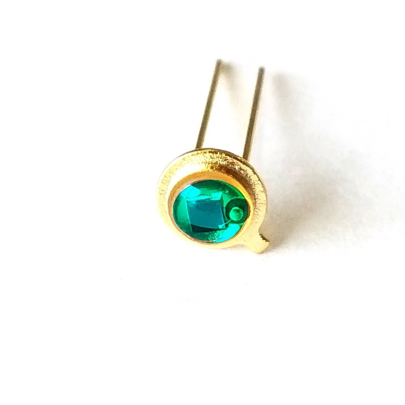
Engineered Hardware & Integrated Sensor Modules
Direct from our onsite-verified Shenzhen manufacturing lines: precision-fabricated multilayer flexible interconnects, optical sensing arrays, advanced thermal control components, and custom electro-mechanical sub-assemblies.
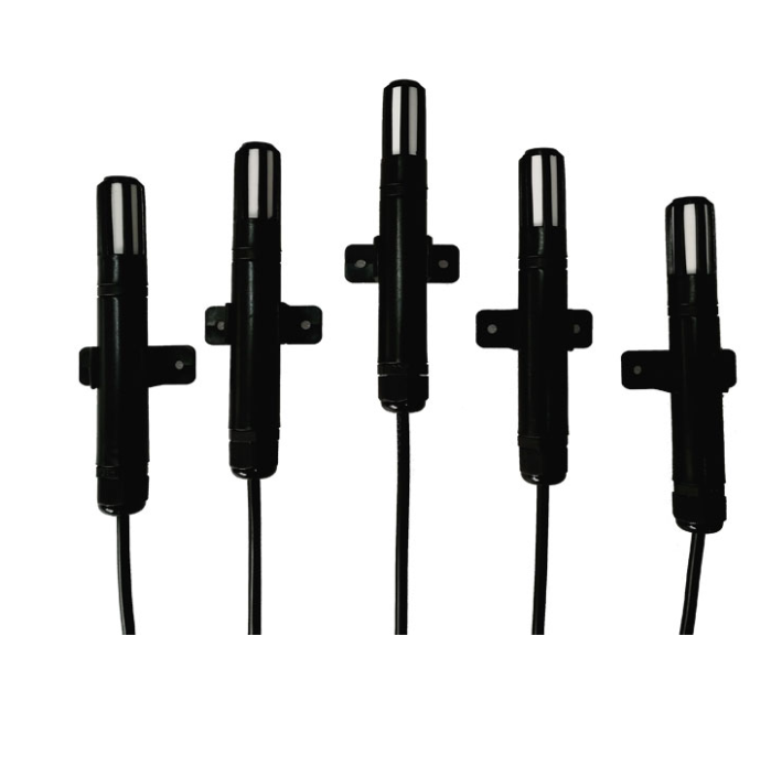
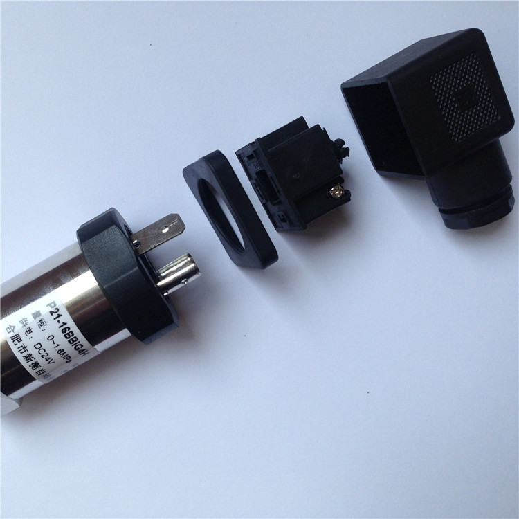

Engineering Authority: Multilayer Flexible PCB Substrate Architecture
As modern mission-critical hardware transitions to lighter, dynamic form factors, multilayer flex circuits (FPCs) solve severe thermal, volumetric, and electromagnetic interference (EMI) bottlenecks across high-frequency applications.
Adhesiveless Polyimide (PI) Cores
Traditional acrylic and modified epoxy adhesive layers exhibit high coefficient of thermal expansion (CTE) mismatches and high dielectric losses at elevated frequencies. We build with premium adhesiveless rolled annealed (RA) copper-clad polyimide laminates (12.5µm to 50µm). This eliminates micro-via fractures during lead-free reflow profiles exceeding 260°C and guarantees continuous dynamic flexing resilience beyond 200,000 cycles.
Adhesiveless Core
Dk 3.2 @ 10GHz
IPC-6013 Class 3
Microvia Drilling & Blind/Buried Routing
Harnessing UV laser ablation systems operating down to 50µm spot sizes, our multilayer FPC production achieves high-density interconnect (HDI) configurations with staggered and stacked blind/buried microvias. Combined with reverse-pulse copper plating, we ensure void-free barrel metallization with 100% coplanar reliability, drastically shrinking trace-to-trace pitch to 40µm/40µm (1.6 mil) for tight BGA packaging.
50µm UV Laser Via
40/40µm L/S
Solid Via Fill
Electromagnetic Shielding & Controlled Z0
To eliminate cross-talk and preserve differential pair signal integrity in multi-gigabit data channels (PCIe Gen 4/5, LVDS, and USB4), our multilayer flex circuits integrate silver paste shielding films or hatched copper ground planes. We deliver strict impedance tolerances (±5% to ±8%) across single-ended 50Ω and differential 90Ω/100Ω geometries, validated through Time-Domain Reflectometry (TDR) reporting.
±5% TDR Control
Silver Shield Film
Faraday Cages
Substrate Engineering Comparison: Dynamic vs. Static Flex Formats
System architects must choose the appropriate flexible printed circuit laminate structure to prevent catastrophic mechanical fracture, dielectric breakdown, or thermal throttling under operating conditions.
| Substrate Architecture | Primary Dielectric & Core | Dynamic Bending Radius | Thermal Endurance (Tg / Td) | Target Applications & Advantages |
|---|---|---|---|---|
| Multilayer Dynamic FPC (4–8 Layers) | Adhesiveless Polyimide (12.5µm–25µm) + RA Copper Foil | ≤ 6× Board Thickness (>250,000 Cycles) | Tg > 280°C | Td > 380°C | Medical endoscopes, aerospace gimbal controls, robotics articulation joints, and folding displays. |
| Rigid-Flex PCB Hybrid (4–16 Layers) | Polyimide Mid-Layers with High-Tg FR-4 Outer Armor | Static / Flex-to-Install (10–12× Thickness) | Tg 170°C (FR-4) / 280°C (PI) | Automotive battery management systems (BMS), avionics computers, compact defense telecommunications. |
| Modified Polyimide (MPI) High-Speed Flex | Low-Loss Modified Polyimide with Smooth Copper | Dynamic & Semi-Dynamic (8–10× Thickness) | Tg > 230°C | Td > 350°C | 5G mmWave antennas, sub-6GHz RF front-end modules, and automotive radar arrays up to 40GHz. |
| Metal-Backed / Aluminum Core Flex | Thin PI Bonded to 5052/6061 Anodized Aluminum | Strictly Planar / Pre-Formed Contour Only | High Thermal Dissipation (1.5–3.0 W/m·K) | High-flux LED automotive headlamps, industrial power converters, and graphics cooler interfaces. |
Procurement Intelligence: Strategic Trends in Multilayer FPC Sourcing
Cross-border procurement directors and hardware engineering leads face rapid technology shifts. Sourcing strategies are moving beyond bare board pricing to total-cost-of-ownership (TCO) models built on supply-chain resilience and automated verification.
Consolidated Turnkey Box-Build
Global OEMs are moving away from fragmented procurement where bare FPCs, SMD passives, micro-connectors, and custom silicone sensors are sourced from separate vendors. Consolidating raw flexible circuit fabrication, BOM procurement, automated pick-and-place assembly, and functional testing under one supplier eliminates vendor-to-vendor blame and lowers defect exposure during lead-free reflow.
BOM Lifecycle & Alternative Sourcing
Supply market unpredictability requires proactive component lifecycle mapping. Leading exporters maintain automated procurement links within the Shenzhen Huaqiangbei and Pearl River Delta electronic ecosystems. When microcontrollers or sensor ICs encounter extended lead times, engineers provide verified drop-in equivalents before initiating solder paste printing.
Demand for Low Dk/Df Substrates
With edge computing, high-bandwidth USB4, and localized AI hardware demanding transfer speeds past 20Gbps, traditional flexible polyimide is being enhanced or replaced by Liquid Crystal Polymer (LCP) and fluoropolymer matrices. These materials keep dielectric loss tangents below 0.002, preventing signal degradation in compact multi-layer assemblies.
Traceability via Laser Direct Marking
Aerospace, automotive, and medical device regulations mandate individual board traceability. Modern fabrication setups employ high-contrast UV laser engraving for micro 2D data-matrix codes directly onto the polyimide coverlay or stiffeners, logging complete laminate lot data, reflow oven thermal curves, and electrical test logs for 5+ years.
Technological Horizons: The Next Phase of Multilayer Flexible Circuits
Flexible printed circuits are evolving from simple point-to-point harness replacements into complex, multifunctional three-dimensional electronic systems.
Additive Semi-Additive Processing (mSAP)
As components shrink toward 0.3mm pitch BGAs and 01005 passives, subtractive chemical etching reaches its physical boundaries due to undercut defects. Next-generation flex circuit manufacturing utilizes modified Semi-Additive Processing (mSAP). By electroplating copper within precise photoresist channels over ultra-thin seed layers, traces achieve vertical, rectangular cross-sections with line/space dimensions down to 20µm/20µm, boosting routing density by 300%.
Embedded Actives & Integrated Passives
To maximize interior space in surgical tools, hearing aids, and aerospace drones, multilayer FPC construction embeds bare silicon dies, thin-film resistors, and planar capacitors directly into intermediate polyimide cores. Laser-drilled microvias connect directly to component termination pads, eliminating external solder joints, cutting parasitic inductance, and boosting shock resistance.
3D Structural & Dynamic Molded Interconnects
The boundary between mechanical housings and internal electronics continues to merge. Multilayer flex circuits are increasingly co-molded or thermoformed with advanced polyimides to match interior curved contours. When paired with localized stainless steel, polyimide, or FR-4 stiffeners, they deliver both rigidity for component mounting and flexible routing across tight mechanical hinge axes.
Frequently Asked Questions: Global Multilayer FPC Sourcing
Detailed technical, quality, and logistics answers addressing common challenges encountered by engineering and procurement teams during quoting and volume manufacturing.
What engineering design rules are critical when laying out dynamic multilayer flex circuits?
For dynamic applications requiring hundreds of thousands of flex cycles, circuits should be laid out along a neutral bend axis. Copper traces should never overlap vertically across adjacent layers (stagger traces instead). Always use Rolled Annealed (RA) copper foil rather than Electro-Deposited (ED) copper, maintain trace paths perpendicular to the bend axis, and avoid plated through-holes (PTH) or microvias within dynamic bend zones. Teardrop all pad-to-trace transitions and apply curved corner fillets instead of 90-degree corners to eliminate localized mechanical stress concentrations.
What is the minimum order quantity (MOQ) and rapid prototype lead time?
We maintain an agile, low-barrier prototyping model. Multilayer flexible PCB prototypes and custom turnkey PCBA runs begin at just 5 pieces to support engineering validation, pilot runs, and functional verification. Rapid prototype turnarounds for 2-to-6 layer standard flexible boards typically ship in 5 to 7 working days following DFM approval, while volume production deliveries range between 12 and 18 working days depending on BOM complexity and layer counts.
Which engineering files and documentation are required for a comprehensive DFM review?
To generate an accurate engineering quote and initiate design-for-manufacturability (DFM) analysis, please provide: (1) Complete Gerber files in RS-274X format or ODB++ databases including drill drawings; (2) Detailed stack-up specifications indicating polyimide dielectric thickness, copper foil weights (0.5oz, 1oz, etc.), and coverlay colors; (3) Stiffener drawings specifying materials (FR-4, aluminum, stainless steel) and bonding methods (PSA vs. thermosetting); (4) BOM detailing manufacturer part numbers for turnkey PCBA; and (5) Pick-and-place centroid coordinates and functional testing parameters.
How do you verify electrical continuity, impedance tolerances, and internal layer alignment?
Every multilayer flexible circuit panel undergoes comprehensive quality verification before shipment: 100% Flying Probe Testing or dedicated Flying Fixture E-testing checks for opens and shorts down to 20V–250V thresholds. Controlled-impedance coupons processed alongside production panels are validated using high-bandwidth Time-Domain Reflectometry (TDR) workbenches. Internal microvia alignment, copper barrel thickness (≥20µm minimum), and resin fill integrity are verified via micro-sectioning and optical metallurgical analysis per IPC-TM-650 specifications.
How does Mivo Electronics ensure component authenticity and manage supply chain shortages?
Located directly in the global electronics manufacturing hub of Shenzhen, China, we source active and passive electronic components exclusively through authorized tier-1 franchised distributors (including Arrow, DigiKey, Mouser) and original component manufacturers. In situations involving unexpected obsolescence or long factory lead times, our components team identifies alternative drop-in parts. Comprehensive datasheets, pin-to-pin footprint comparisons, and parametric impact analyses are sent for your written engineering sign-off before purchase.
Shenzhen Manufacturing Authority: Precision, Scale & Reliability
Shenzhen Mivo Electronics Co., Ltd. operates an onsite-verified electronics production, turnkey assembly, and sensor manufacturing facility in Yuanshan Street, Longgang District, Shenzhen. Our multidisciplinary engineering team combines modern automated SMT placement, high-precision multilayer flex circuit fabrication, and specialized sensor production to serve industrial OEMs worldwide.
- Independently Audited & Onsite Verified: Factory premises, workforce capacity, and trade authenticity verified by Alibaba and third-party inspectors.
- 8+ Years Global Export Track Record: Consistent export operations serving customers in North America, Western Europe, Southeast Asia, and South America with a verified 4.7/5.0 buyer satisfaction score.
- Comprehensive Cross-Discipline Portfolio: Single-source delivery of Multilayer FPCs, Rigid-Flex, Aluminum Core MCPCBs, Laser SMT Stencils, Custom Sensors (PT100, SHT30, Optical), and Membrane Switch panels.
Audited Corporate Profile
Operational Base
Shenzhen, Guangdong, China
Verified Establishment
2016 (Onsite Confirmed)
Core Facility Area
101 – 500 m²
Engineering Staff
51 – 100 Skilled Personnel
Compliance System
RoHS, REACH, IPC-6013 Class 2/3
Minimum Order Line
Starts from 5 PCS (PCBA & Flex)
Launch Your Multilayer Flex Circuit Project Today
Submit your Gerber designs, stack-up parameters, or custom BOM to our Shenzhen engineering team. We deliver thorough DFM reports, impedance simulations, and competitive manufacturing quotes within 24 hours.