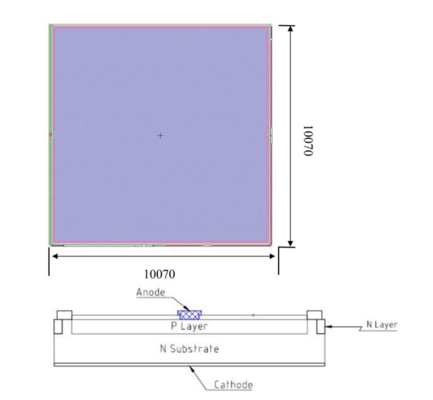
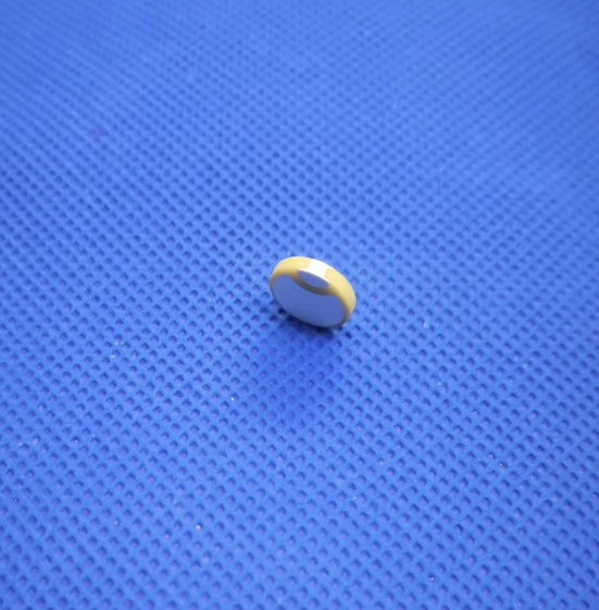
Q1: What are the key dimensions and type of this photocell chip?
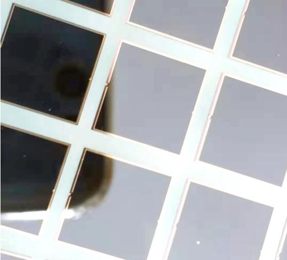
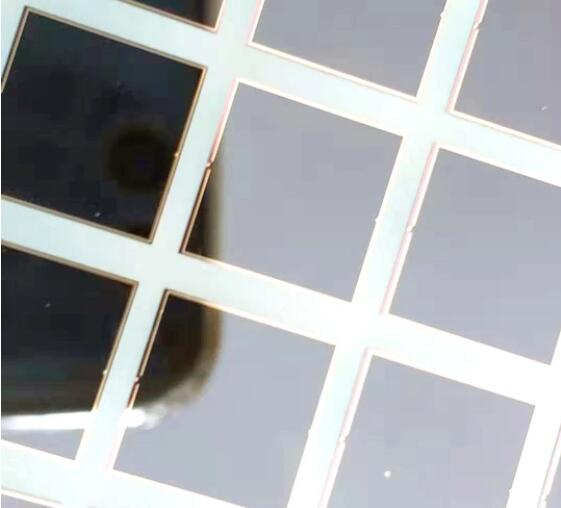
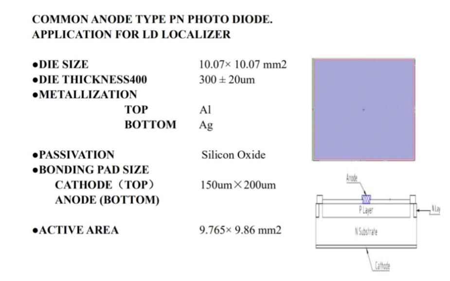
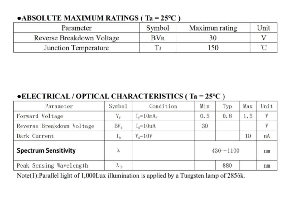
This component is a 10*10 mm bare silicon wafer designed as a linear silicon photodiode chip, utilizing a common anode structure for PN photo diode integration.
Q2: What does "Common Anode" mean for this PN photodiode?
A common anode configuration means that the positive terminal (anode) is shared across the chip structure, making it ideal for unified circuit grounding or multi-element sensor routing.
Q3: Can this bare silicon wafer be used for SGPIN400 applications?
Yes, the chip is specifically compatible with SGPIN400 configurations, delivering high sensitivity and linear response for optical sensing systems.
Q4: Do you accept bulk procurement and custom dimensions?
Yes, both volume bulk orders and custom service orders are fully supported to match specialized electro-optical requirements.
Q5: What precautions should be taken when handling bare silicon wafers?
Bare silicon wafers are sensitive to electrostatic discharge (ESD) and surface contamination; handle using cleanroom tweezers in an anti-static, dust-free environment.