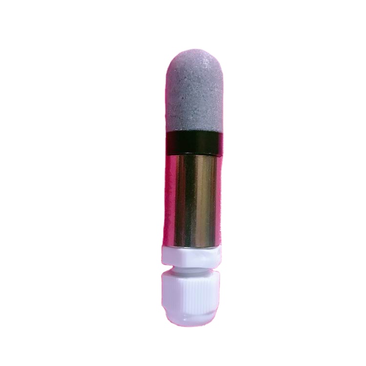
Waterproof PE Temperature & Humidity Sensor Shell
SHT10, SHT11, SHT20, SHT30 compatible housing. Sintered PE porous filter head with high anti-condensation sealing.
Explore our core portfolio of wafer-level photodiodes, sensor housings, and electro-mechanical modules engineered to rigorous European tolerances.
SHT10, SHT11, SHT20, SHT30 compatible housing. Sintered PE porous filter head with high anti-condensation sealing.
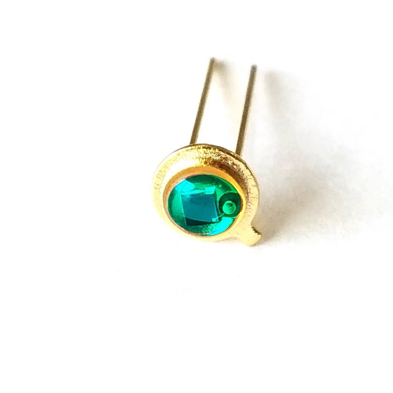
Fast response, 450nm optimized visible/NIR band silicon photocell housed in a hermetically sealed low-noise TO-46 can.
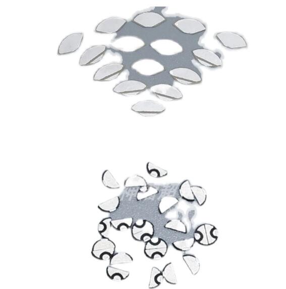
Profiled hyperchromatic waveguide transducer for non-destructive ultrasonic acoustic emission & structural resonance testing.
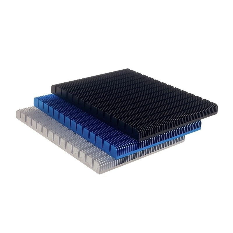
Precision extruded aluminum cooler with industrial thermal adhesive tape for high-density optoelectronics, SSD, CPU & PCBA dissipation.
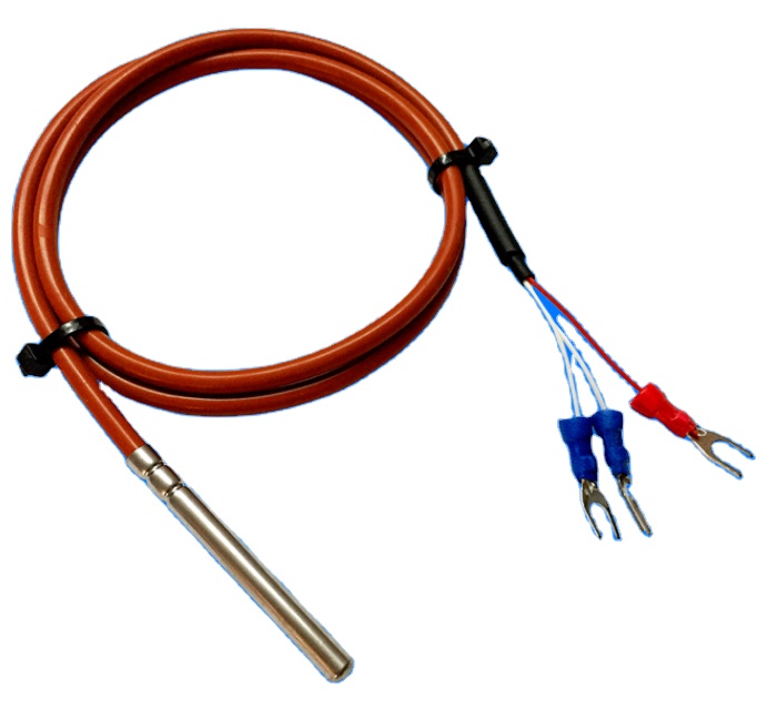
Class A platinum resistor, 3-wire system, 1-5m high-purity silicone gel coat. Waterproof, oil-proof cryogenic & thermal resilience.
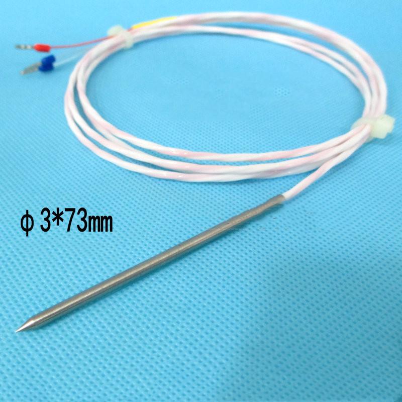
Needle-point penetration tip (PT100A/PT1000). Rapid thermal equilibration for bioprocessing, cold-chain, and lab immersion test beds.
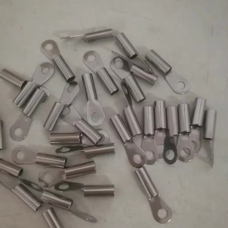
Surface-mount 4mm screw eyelet lug fabricated from stamped 201 stainless steel. Superior heat coupling for battery packs & motor enclosures.
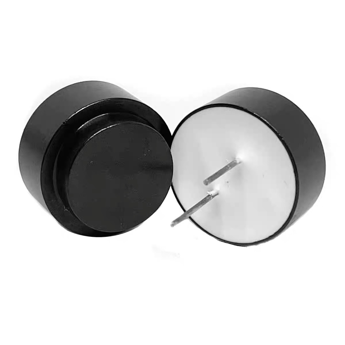
Integrated transceiver module for automotive park assist, robotics rangefinding, and IoT liquid level telemetry in harsh ambient environments.
Bare silicon photodiode wafers represent the foundational building block for modern optoelectronic transceivers, radiation detectors, analytical spectrometers, and industrial laser diagnostics. Unlike standard pre-packaged components (e.g., molded plastic epoxy or surface-mount leaded packages), procuring at the bare wafer or diced unmounted die level affords photonic systems engineers complete control over optical coupling geometry, parasitic capacitance, thermal dissipation paths, and sub-nanosecond rise-time tuning.
Shenzhen Mivo Electronics exports raw, unmounted monocrystalline planar diffusion and PIN silicon photodiode wafers engineered from ultra-pure, high-resistivity float-zone (FZ) or Czochralski (CZ) ingots. Featuring planar passivated junctions, thermally grown silicon dioxide (SiO2) or specialized silicon nitride (Si3N4) anti-reflective coatings (ARC), our wafers maximize spectral responsivity across the ultraviolet (UV), visible (VIS), and near-infrared (NIR) wavelengths (190 nm to 1100 nm). Each wafer is subjected to micron-level wafer thickness mapping, laser-scribed dicing grid preparation, and cleanroom automated probing to ensure sub-nanoampere dark currents and high shunt resistance across all functional dice.
Fabricated with an intrinsic high-resistivity layer between p+ and n+ regions, resulting in an ultra-wide depletion region at low reverse bias. Delivers cutoff frequencies in excess of 1 GHz with sub-nanosecond rise/fall transients.
Customizable dielectric anti-reflective coatings tuned specifically for 405nm (blue laser), 650nm (visible red), or 850/905nm (NIR LiDAR/rangefinding), achieving quantum efficiencies surpassing 85% with minimal surface recombination.
Supplied on UV dicing tape, Grip-Ring carriers, or conductive Gel-Pak trays. Dice are fully metallized on front (anode wire-bondable Au or Al) and backside (cathode solderable Au/Sn or conductive epoxy compatible) for hybrid micro-assembly.
For research teams and microelectronic assembly lines throughout the Greater Stockholm region, selecting the correct wafer thickness, active area geometry, and doping profile directly dictates the optical noise floor (NEP) and dynamic range of the terminal device. The table below outlines our standard exporter catalog grades:
| Wafer / Die Series | Active Area Geometry | Spectral Peak | Dark Current (Id @ Vr) | Junction Capacitance | Primary Industrial Use |
|---|---|---|---|---|---|
| MIVO-SPD-UVB UV Enhanced | 1.0 × 1.0 mm to 10 × 10 mm | 360 nm (200–400 nm) | < 50 pA @ 0V | 120 pF / cm² | Biotech fluorescence, ozone sensing, water sterilization monitors |
| MIVO-SPD-VIS High Shunt | Round / Square (Custom Die) | 550 nm (Photopic match) | < 20 pA @ 10mV | 350 pF / cm² | Nordic precision optical lux meters, colorimetry, camera sensors |
| MIVO-PIN-FAST High Speed | 0.5 × 0.5 mm or 1.2 mm² | 850 / 905 nm | < 0.5 nA @ 10V | 1.8 pF @ 10V | Autonomous driving LiDAR, time-of-flight (ToF), fiber optic hubs |
| MIVO-QUAD-POS Quadrant Array | Segmented 4-Quadrant (Gap 40μm) | 650 nm / 850 nm | < 100 pA / quadrant | 15 pF / segment | Laser beam alignment, multi-axis target tracking, robotics deflection |
Stockholm is recognized across the European Union as a powerhouse for photonics innovation, automated green shipping, precision robotics, and MedTech design. Often centered around northern hubs like Kista Science City (Sweden's premier ICT and electronics cluster) and research epicenters like KTH Royal Institute of Technology and Karolinska Institutet, local hardware innovators require agile, high-precision semiconductor supply lines.
As Swedish original equipment manufacturers (OEMs) shift toward localized green-tech initiatives, life sciences, and Industry 4.0 automation, off-the-shelf catalog photodiodes frequently prove too bulky, thermally inefficient, or acoustically restricted. Shenzhen Mivo Electronics bridges this gap by acting as a direct engineering-to-production exporter, supplying bare photodiode wafers, custom hybrid ceramic sub-mounts, and matched PCBA sensor assemblies with uncompromised traceability.
Stockholm's life-science cluster utilizes custom bare photodiode dice for point-of-care microfluidic chips, in-vitro blood gas analyzers, and spectrophotometers demanding near-zero dark current noise floor.
Integrated photodetection dice powering next-generation optical transceivers, dense optical cross-connects, and free-space optics (FSO) links across Nordic cold-climate wireless infrastructure.
Coupling bare photocells and SHT30/PT100 sensors into remote meteorological stations, heat pump optimization arrays, and forestry canopy solar-penetration logging equipment.
High-speed pulse detection for laser curtain safety, precision alignment in Swedish automated mining loaders, and autonomous harbor logistics around the Baltic Sea coastline.
Navigating cross-border component procurement between Sweden and China requires absolute reliability, rigorous technical vetting, and rapid turnarounds. Shenzhen Mivo Electronics Co., Ltd. is not merely a broker; we are an onsite-verified manufacturer established in Shenzhen's world-class microelectronics hub, operating complete production, inspection, and component mounting facilities.
Our facilities have successfully passed independent third-party and Alibaba.com onsite audits. With over 8 consecutive years of transparent global trade history and a 4.7/5 verified buyer score, we assure Swedish buyers full accountability.
Eliminate multiple middleman vendors. We supply bare photodiode wafers, solder paste stencils, multilayer and aluminum-core PCBs, SMT component mounting, and custom probe wire harnesses directly from a unified project team.
We empower Swedish hardware startups and corporate R&D groups with custom prototypes starting from just 5 pieces for PCBA and low MOQ on bare photodiode dice, enabling agile bench testing before scaling into container-volume production.
Direct answers addressing the technical, regulatory, logistical, and commercial inquiries common among Swedish procurement directors and hardware engineering teams.
Whether you require unmounted silicon photodiode wafers, diced array wafers, or complete turnkey PCBA sensor integrations, our technical sales engineers are ready to review your mechanical drawings and Gerber packages.