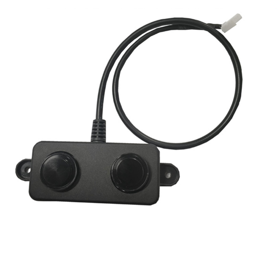
Acoustic & Ranging
Serving original equipment manufacturers (OEMs), precision engineering laboratories, and sensor assembly houses throughout Milan, Turin, Bologna, Florence, and Genoa. Discover our high-yield unpackaged bare photodiode wafers, planar photodetector elements, and complementary sensing modules.
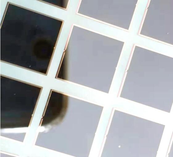
In optical metrology and high-speed industrial feedback loops, packaged optoelectronic sensors often present severe physical bottlenecks: parasitic packaging inductance, high profile form factors, thermal mismatch between hermetic headers and ceramic carriers, and optical attenuation from uncalibrated epoxy or glass windows. For advanced research centers and manufacturers across Italy, bare silicon photodiode wafers (unpackaged dice) represent the definitive engineering substrate for hybrid multi-chip modules (MCM), chip-on-board (COB) architectures, and ultra-compact optical receiver assemblies.
Our bare wafers utilize ultra-pure, high-resistivity Float Zone (FZ) and Czochralski (CZ) crystalline silicon, grown in ⟨100⟩ or ⟨111⟩ crystal orientations. By strictly regulating background dopant concentrations (n-type phosphorus or p-type boron), we achieve wide intrinsic depletion widths under reverse bias, guaranteeing high charge collection efficiency across both visible and near-infrared (NIR) spectra.
Thermally grown silicon dioxide (SiO&sub2;) combined with plasma-enhanced chemical vapor deposition (PECVD) silicon nitride (Si&sub3;N&sub4;) creates dual-layer anti-reflective coatings (ARC). This passivation suppresses dangling surface bonds, eliminating surface recombination velocities and cutting dark current (Id) to picoampere levels at room temperature.
Anode contacts feature pure titanium/platinum/gold (Ti/Pt/Au) or aluminum-silicon-copper (Al-Si-Cu) metallization suitable for high-speed thermosonic gold ball bonding or ultrasonic aluminum wedge bonding. Cathode back-metallization (Ti/Ni/Ag or Au) guarantees low contact resistance during eutectic die-attach or silver glass paste mounting.
| Parameter | Standard Silicon PIN Wafer | UV-Enhanced Bare Wafer | NIR-Enhanced High-Speed Die | Testing Conditions |
|---|---|---|---|---|
| Spectral Range (λ) | 400 nm – 1100 nm | 190 nm – 1100 nm | 700 nm – 1100 nm | T = 25°C, Sensitivity cutoff |
| Peak Responsivity (R) | 0.62 A/W @ 900 nm | 0.18 A/W @ 254 nm | 0.68 A/W @ 980 nm | VR = 5V |
| Dark Current (Id) | ≤ 0.5 nA / mm² | ≤ 0.2 nA / mm² | ≤ 1.2 nA / mm² | VR = 10V, 100% Wafer Probed |
| Junction Capacitance (Cj) | 12 pF / mm² | 25 pF / mm² | 3 pF / mm² | VR = 10V, f = 1 MHz |
| Rise Time (tr) | 5 ns | 12 ns | 0.8 ns | RL = 50 Ω, VR = 20V |
| Wafer Thickness | 380 μm ± 15 μm | 300 μm ± 10 μm | 200 μm ± 10 μm | Polished / Chemical Etched |
Italy represents Europe’s second-largest manufacturing powerhouse, defined by specialized regional clusters that require tailored optoelectronic components. Our bare silicon photodiode wafers, custom photocell chips, and associated sensors are deployed directly into key Italian technological ecosystems:
Centering on Bologna, Modena, and Parma, Italian automatic packaging machinery builders require high-speed optical registration arrays. Unpackaged photodiode chips are integrated into custom multi-channel transimpedance sensor bars to verify blister pack completeness, print alignment, and optical liquid level verification at speeds exceeding 1,200 packages/minute.
In the industrial belts of Milan, Brescia, and Turin, machine tool fabricators and electric drivetrain Tier-1 suppliers embed bare silicon photodiodes into high-precision absolute rotary encoders, laser welding seam-trackers, and EV battery arc fault optical detection systems that integrate seamlessly with our NTC battery temperature sensors.
Europe's foremost biomedical district in Mirandola utilizes our UV-sensitive bare silicon photodiode wafers for clinical in-vitro diagnostic (IVD) instruments, microfluidic optical absorption flow cells, and hemodialysis blood leakage optical monitors that require low noise and zero cross-talk.
Precision optics manufacturers in Florence and CNC tooling builders in Padua and Vicenza incorporate bare 10×10 mm silicon photocell chips for multi-axis laser beam profiling, optical micrometer gauges, and chromatic confocal displacement probes where minimal thermal drift is critical.
The procurement of photodetector elements in Italy is experiencing a profound technological transition, driven by institutional modernization plans, technological convergence, and strict European sustainability mandates.
The Italian government's Piano Transizione 5.0 incentivizes smart manufacturing systems that combine digitization with measured energy consumption reductions. Italian automation firms are moving toward edge-sensorized machines, requiring custom optoelectronic dies that can be mounted directly on PCB control surfaces alongside local processing microcontrollers to minimize power consumption.
To stay competitive against global equipment suppliers, Italian instrument makers are replacing discrete canned sensors (e.g., TO-5, TO-18) with System-in-Package (SiP) and Chip-on-Board (COB) topologies. Purchasing 100% probed bare silicon wafers allows Italian factories to achieve sub-millimeter profiles, minimize parasitic board capacitance, and eliminate expensive assembly labor.
Following supply chain disruptions, Italian engineering procurement teams are bypassing regional broker markups, opting instead to establish direct relationships with verified semiconductor and PCB/sensor manufacturers. Direct factory engagement enables tailored dicing streets, custom wafer thicknesses, and complete technical visibility from ingot to finished die.
Shenzhen Mivo Electronics Co., Ltd. combines specialized semiconductor wafer processing with comprehensive PCB fabrication and turnkey electronic assembly. While pure silicon foundries demand prohibitively large MOQs and PCBA contractors lack optoelectronic cleanroom expertise, we bridge the gap with agile, verified manufacturing solutions tailored to overseas buyers.
Our manufacturing facilities in Yuanshan Street, Shenzhen, have successfully passed rigorous third-party onsite verifications by international inspection agencies. With an established operation since 2016 and an 8-year verified track record on global platforms, our legal status and production capacities are fully certified.
Wafers are handled in Class 1,000 / Class 10,000 cleanroom environments. We provide complete backend dicing services: un-diced full wafers, dice sawn on UV-release blue tape rings (Disco compatible), or individually sorted defect-free dice packed in antistatic Gel-Pak trays with wafer probing map files.
Beyond raw silicon, Mivo Electronics operates surface mount (SMT) and through-hole assembly lines. We can take your bare photodiode wafer and execute precision die-attach, micro-wire bonding, optical encapsulation, and peripheral signal conditioning on multilayer FR-4 or ceramic PCBs from prototype runs of 5 pieces.
Addressing key technical, compliance, logistical, and commercial inquiries commonly raised by Italian buyers.
Whether you need catalog unpackaged silicon photodiode wafers, custom quadrant detector dies, or turnkey chip-on-board assembly for your Italian manufacturing plant, our senior optoelectronic engineers are ready to assist. Request comprehensive technical datasheets, wafer maps, and quotation packages today.
Get Catalog