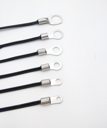
Automotive Grade
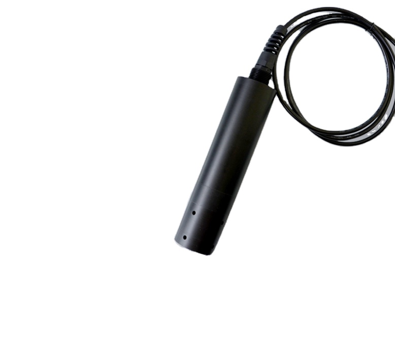
New Energy Automobile Power Battery Temperature Sensor NTC 100K Temperature Probe B4150
● In Stock
Inquire Now
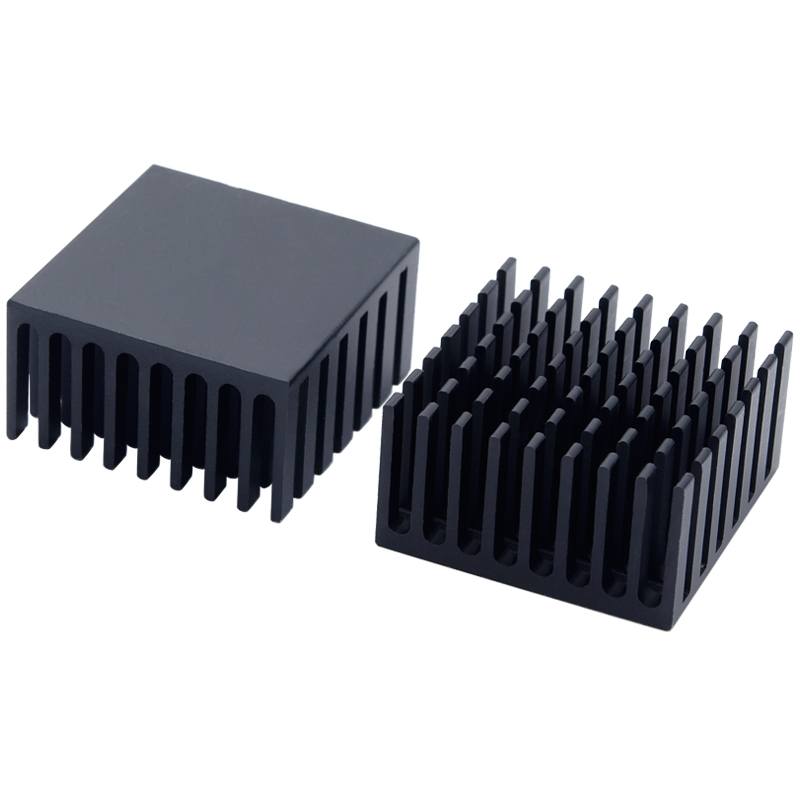
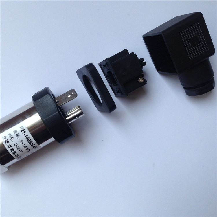
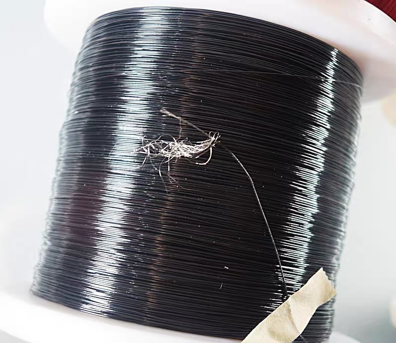
Direct supply of photodiode wafers, temperature probes, structural heat sinks, and auxiliary connectivity modules engineered for precision deployment.
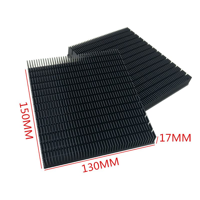
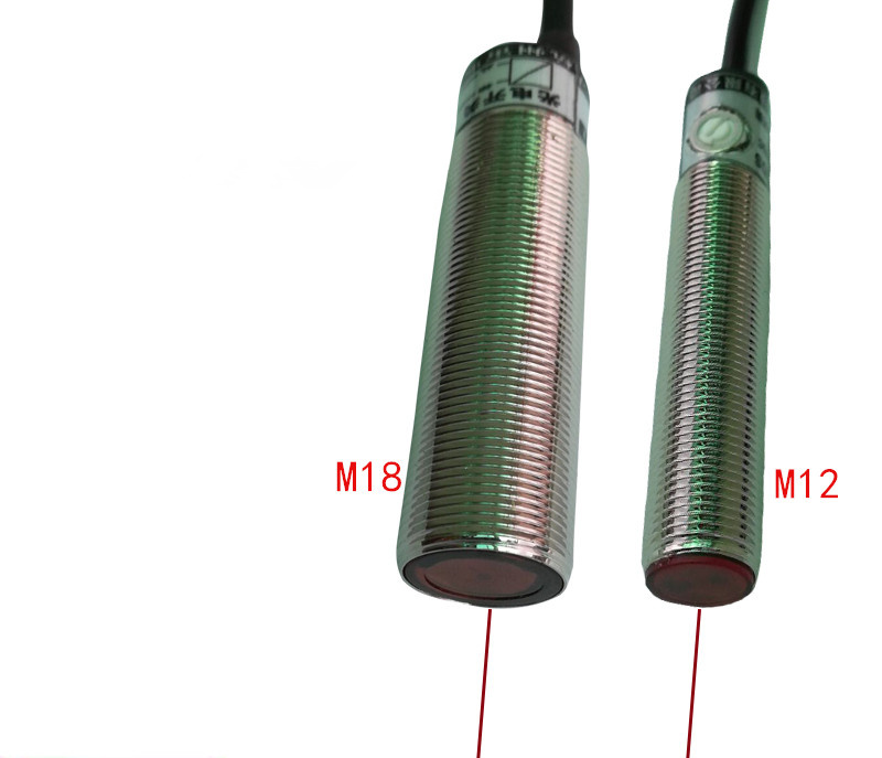
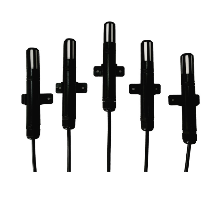
In the evolving landscape of solid-state photonics, bare silicon photodiode wafers serve as the fundamental optoelectronic transducer substrate. Unlike encapsulated discrete photodetectors, bare wafer dies offer advanced electronic device fabricators, system-in-package (SiP) integrators, and hybrid optical circuit manufacturers ultimate architectural freedom. By delivering un-diced full wafers, partially sawn wafer rings, or pick-and-place bare dice, Shenzhen Mivo Electronics Co., Ltd. supplies high-responsivity, low-dark-current optoelectronic silicon direct to engineering clusters globally, including Cartago's rapidly advancing high-technology and medical device manufacturing ecosystems.
Our bare silicon photodiode wafers utilize high-resistivity float-zone (FZ) and polished Czochralski (CZ) crystalline silicon substrates. Through precise planar diffusion technology, specialized anti-reflective passivation layers (such as LPCVD Silicon Nitride - Si3N4 or Thermal SiO2), and optimized metallization (Ti/Ni/Au or Al/Si/Cu ohmic contacts), our dies achieve remarkable quantum efficiency spanning ultraviolet-enhanced (200–400 nm), visible spectrum (400–750 nm), and extended near-infrared (NIR up to 1100 nm) wavelengths.
Information Gain Metric: Standard commercial photodiodes introduce packaging parasitic capacitances (0.8–2.5 pF) and thermal boundary degradation via transfer-molded epoxy. Our bare-die integration directly yields junction capacitance reductions exceeding 65%, achieving sub-nanosecond rise times (tr < 0.9 ns) under modest reverse bias voltages (VR = 5V to 15V), quintessential for high-frequency optical transceivers and compact analytical spectrometers.
Engineered with micro-thin active depletion layers tailored to eliminate carrier transit delays, driving rise/fall speeds required for high-speed pulse detection.
Passivated guard-ring architectures severely suppress surface leakage currents, yielding dark current densities below 0.1 nA/cm² at ambient 25°C.
Tunable anti-reflection thin-film coatings configured for high quantum efficiency across UV-visible (300-700nm) and NIR telemetry wavelengths (850-1064nm).
The following performance matrix defines the base structural and electrical metrics standard across our bare silicon wafer product families, fully configurable to custom fabrication prints:
| Physical / Electrical Parameter | Standard Photodiode Die Series | High-Speed PIN Wafer Series | UV-Enhanced Photodiode Series |
|---|---|---|---|
| Wafer Diameters & Thickness | 100 mm / 150 mm (4" / 6"), 380 ± 20 µm | 150 mm (6"), 300 ± 15 µm (Thinned opt.) | 100 mm / 150 mm, 380 ± 25 µm |
| Substrate Type & Resistivity | CZ / N-type (100) / 10–50 Ω·cm | FZ / High-Res N-type > 2000 Ω·cm | FZ / P-type or N-type > 500 Ω·cm |
| Active Area Geometries | 0.5×0.5 mm² to 10×10 mm² (Custom Matrix) | 0.2×0.2 mm² to 3×3 mm² Linear Arrays | 1×1 mm² to 10×10 mm² Single Quadrants |
| Peak Responsivity (λp) | 0.62 A/W @ 900 nm | 0.58 A/W @ 850 nm | 0.18 A/W @ 254 nm / 0.45 A/W @ 632 nm |
| Dark Current (Id @ VR = 5V) | ≤ 0.5 nA (Typ. 0.1 nA @ 25°C) | ≤ 0.2 nA (Typ. 0.05 nA @ 25°C) | ≤ 0.8 nA (Typ. 0.2 nA @ 25°C) |
| Junction Capacitance (Cj) | 15 pF / mm² @ 0V | 1.2 pF / mm² @ VR = 10V | 18 pF / mm² @ 0V |
| Top Metallization (Anode/Cathode) | Al / Si / Cu (Wire-bondable Au available) | Ti / Pt / Au (Au wire-bonding & flip-chip) | Pure Aluminum (Optimized UV Transmission) |
| Backside Metallization | Gold (Au) / Silver (Ag) Eutectic Solderable | Ti / Ni / Au (Conductive Epoxy / Solder) | Au / Sb (N-type) or Au / Zn (P-type) |
Strategic deployment within Cartago’s Free Trade Zones (Zonas Francas) driving the convergence of precision medical devices, aerospace sensors, and advanced microelectronics.
Integration into minimally invasive diagnostic catheter tips, in-vitro blood oximetry modules, and laser ablation surgical feedback monitors across Cartago industrial clusters.
Supplying raw diced chips on blue tape rings designed for automated vacuum pick-and-place and wedge/ball thermosonic gold-wire bonders in ISO Class 7/8 facilities.
Equipping Cartago's high-throughput food inspection (coffee/produce color sorting) with multi-element silicon linear arrays exhibiting broad-spectrum optical responsivity.
Radiation-tolerant, high-resistivity silicon substrates engineered for orbital orientation sensors, sun sensors, and optical inter-satellite links assembled by regional aerospace suppliers.
Cartago has rapidly transformed from Costa Rica's historical colonial capital into a focal center for the Americas' semiconductor nearshoring initiative. Propelled by the U.S. CHIPS Act collaboration frameworks and substantial foreign direct investment into parks such as Zona Franca La Lima and Parque Industrial Cartago, regional production has shifted decisively toward advanced microelectronics assembly, test, and packaging (ATP).
This industrial evolution creates critical requirements: Tier-1 and Tier-2 manufacturers located in Cartago can no longer rely on rigid catalog components with 26-week lead times. Engineering teams require agile foundry partners capable of supplying raw optoelectronic wafer stock, customized anti-reflective stack profiles, and rapid prototyping runs that mesh smoothly with high-precision die-bonding equipment. Shenzhen Mivo Electronics fills this operational void by providing direct cleanroom fabrication flexibility combined with agile Shenzhen supply velocity.
Combining Shenzhen's agile semiconductor supply chain with stringent European and North American quality verifications.
Unlike raw silicon suppliers who stop at wafer slicing, Mivo pairs bare photodiode dies directly with our in-house turnkey PCBA, SMT stencil production, custom aluminum heat sink extrusion, and sub-system testing.
Our manufacturing plant in Yuanshan Street, Shenzhen, has passed physical onsite checks by international inspection agencies and Alibaba.com auditors. Production capacity, employee scale, and legal standing are fully validated.
Every batch of silicon wafers, thermistors, coaxial lines, and transducers undergoes incoming wafer mapping, surface contamination control, and transparent manufacturer part number verification.
Addressing compliance, packaging, cold-chain transport, and technical specs for engineers and purchasing agents in Cartago.