High-Density Interconnect (HDI) Architectural Demands in Industrial Central America
Bridging Shenzhen's Premier PCB Fabrication & Turnkey PCBA Infrastructure with the Rapidly Modernizing Industrial and Export Free Zones of Choloma, Cortés
The manufacturing ecosystem of Choloma, Honduras—situated at the core of the Sula Valley economic nexus—is undergoing a profound transformation. Long renowned as an export powerhouse for advanced textiles, synthetic fabrics, garment manufacturing (maquiladoras), and automotive wire harness assemblies under the Zonas Libres (ZOLI) framework, Choloma's industrial facilities are pivoting rapidly toward Industry 4.0 automation, edge computing, smart logistics telemetry, and localized electro-mechanical control. As machinery across local plants integrates complex robotic controllers, high-speed vision inspection systems, intelligent motor actuators, and environmental wastewater monitoring, standard through-hole and conventional multi-layer printed circuit boards (FR-4) are no longer sufficient to meet modern thermal, electrical, and spatial constraints.
Modern high-speed edge devices, robotic micro-controllers, and multi-sensor IoT modules necessitate High-Density Interconnect (HDI) PCBs. HDI architectures utilize microvia technology, sequential build-up (SBU), blind and buried vias, and micro-trace routing under 4 mils (0.10mm) to dramatically reduce circuit board surface area while exponentially increasing electrical performance, signal integrity, and high-frequency RF transmission. For procurement engineers, plant maintenance directorships, and hardware innovators in Choloma, finding a trusted, onsite-verified manufacturing partner capable of executing sub-millimeter component placement and true high-density microvia fabrication is critical to eliminating production downtime and accelerating industrial deployment.
| Engineering Parameter | Standard Multilayer PCB | Mivo Advanced HDI PCB (1+N+1 to Any-Layer) | Impact on Choloma Industrial Deployments |
|---|---|---|---|
| Via Architecture | Mechanically drilled through-hole (min. 0.20mm) | Laser Microvias: Blind, Buried, Staggered, Stacked (0.075mm - 0.10mm) | Allows 60% board footprint compression in automated machine controllers |
| Min. Line Width / Spacing | 4 mil / 4 mil (0.10mm / 0.10mm) | 2.5 mil / 2.5 mil (0.065mm / 0.065mm) ultra-fine pitch | Facilitates fine-pitch 0.4mm BGA routing for ARM/FPGA processing engines |
| Thermal Conductivity & Tg | Standard FR-4 (Tg 130–140°C, 0.3 W/m-K) | High-Tg Shengyi/ITEQ (Tg 170–180°C) + Heavy Copper & Aluminum MCPCB | Withstands severe ambient temperature & thermal cycling in textile dyeing floors |
| Via-in-Pad Protection | Tented or non-conductive masked | VIPPO (Via-in-Pad Plated Over) with planar copper capping | Guarantees zero solder voiding under complex SMT power driver packages |
| Surface Finishes (Industrial) | HASL / Lead-Free HASL | ENIG (Electroless Nickel Immersion Gold), ENEPIG, Immersion Silver | Superior corrosion resistance against acidic air & humidity in tropical wet zones |
Shenzhen Mivo Electronics Co., Ltd. operates at the forefront of this technological shift. Backed by verified fabrication facilities in Shenzhen, China—the undisputed global capital of electronics hardware—our engineering infrastructure supports rapid-turn prototype engineering from 5 pieces to full-scale volume manufacturing. We deliver complete vertical turnkey execution: from native Gerber and CAM validation (DFM) through multilayer precision copper lamination, microvia laser ablation, surface-mount component placement, functional testing, and turnkey industrial sensor integration.
Any-Layer & Sequential Buildup
Delivering 1+N+1, 2+N+2, and Any-Layer ELIC (Every Layer Interconnect) stackups for extreme density computing, high-speed telemetry gateways, and compact industrial vision systems.
Controlled Impedance Matching
Strict TDR impedance tolerance within ±5% to ±7% across high-speed differential pairs (PCIe, USB 3.2, Ethernet 1000Base-T, RS485 Modbus) ensuring crystal-clear industrial communication.
Comprehensive DFM/DFA Verification
Every engineering release is pre-screened with automated Valor Genesis DFM algorithms, identifying copper necking, acid traps, and thermal relief anomalies before raw copper etching begins.
High-Reliability Electronics Applications in Choloma & Cortés Corridor
Custom-Engineered Hardware Solutions Addressing Real-World Operational Demands Across Honduras's Manufacturing Core
Automated Textile & Apparel Plant Control
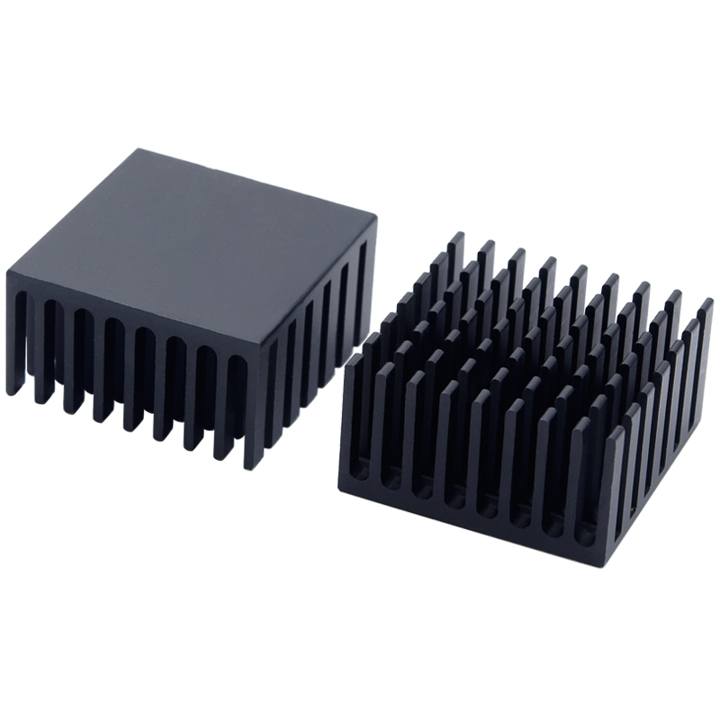
Choloma's massive spinning, knitting, and finishing factories run 24/7. Modern circular knitting machinery and industrial sewing hubs rely on our multi-layer control PCBA integrated with our 28x28x15mm aluminum heatsinks and B3SE tactile switches, providing resilient motor control in lint-heavy, elevated-temperature factory conditions.
Industrial Wastewater Treatment & Dying Vats
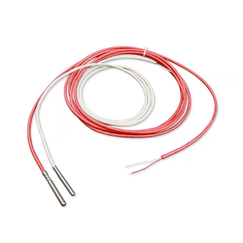
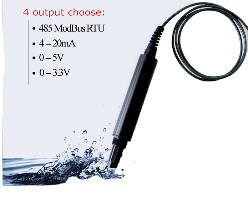
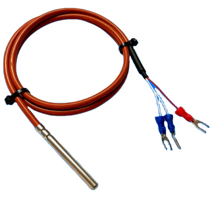
Environmental compliance requires continuous, automated chemical tracking. Our DOS-600 digital dissolved oxygen probes and high-accuracy PT100/PT1000 platinum RTD sensors connect into ruggedized HDI interface boards, resisting severe corrosive chemicals and wet environments in local effluent filtration plants.
Automotive Sub-Assembly & Wire Harnessing
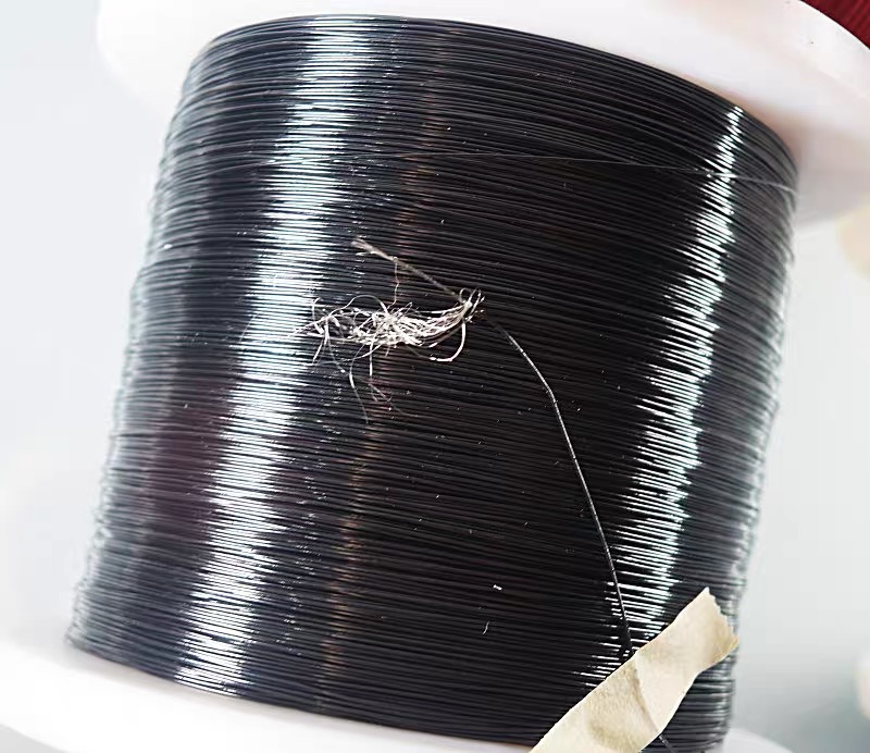
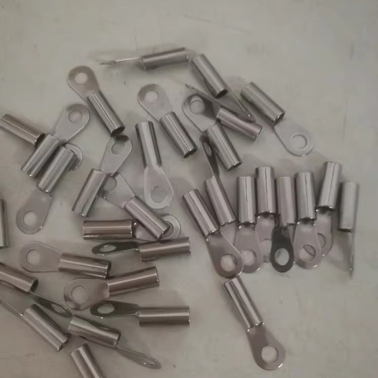
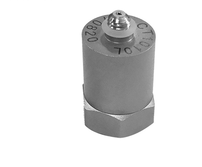
As tier-1 and tier-2 automotive wire harness facilities expand in the Cortés region, our 36AWG ultra-fine 50-ohm micro-coaxial cables, piezoelectric vibration accelerometers (CT1010L), and custom thermocouple terminals supply rigorous telemetry, quality verification rigs, and in-vehicle electronic assemblies.
Localized Technological & Economic Trends in Choloma's Industry
The northern corridor of Honduras, particularly the municipality of Choloma stretching towards Puerto Cortés, represents the most strategically vital industrial gateway in Central America. With direct deep-water port access just 30 miles north at Puerto Cortés, local manufacturers operate under rapid turnaround expectations for exports destined for the United States, Mexico, and South American markets. The rapid infusion of automated sewing platforms, digital fabric printing, and high-speed sorting facilities has exposed a notable vulnerability: dependency on obsolete, low-reliability replacement boards.
To maintain zero-unplanned-downtime quotas, facility operators in Choloma are migrating away from spot-order regional brokers and engaging directly with primary manufacturers in Shenzhen. By establishing direct-to-factory engineering pipelines for FR-4 multilayer boards, metal-core aluminum boards (MCPCB), flexible circuits (FPC), and turn-key assembled controllers, local enterprises reduce component obsolescence risks, gain full traceability down to individual IC batch codes, and achieve unit-cost savings exceeding 35% compared to North American or domestic distribution markups.
Shenzhen Mivo Electronics: Why Global Importers Trust Our Lines
Onsite-Verified Manufacturing Infrastructure Engineered for Seamless Turnkey Assembly & International Traceability
Independent Onsite Verification
Our manufacturing facilities and legal business status in Yuanshan Street, Shenzhen have been verified on-site by international third-party certification authorities and Alibaba.com examiners.
Shenzhen Supply Chain Density
Located in the silicon core of China, we provide transparent BOM sourcing across franchised distributors and primary semiconductor foundries, eliminating counterfeit risks entirely.
Full Vertical Spectrum
Eliminate multi-vendor friction. We deliver bare multi-layer/HDI boards, laser-cut SMT stainless stencils, high-precision component placement, firmware flashing, and matching custom sensor probes.
Strict Quality Assurance
Standard protocols incorporate automated optical inspection (AOI), X-ray BGA void validation, in-circuit testing (ICT), cross-section micro-sectioning, and complete burn-in cycling.
End-to-End Turnkey PCBA & Custom Sensor Manufacturing Roadmap
A Structured, Transparent Engineering Sequence Engineered to Provide Full Assurance from Shenzhen to Choloma
01. Comprehensive DFM & Gerber Audit
Every incoming Gerber (RS-274X, ODB++) package is rigorously screened for trace clearance, copper weight fidelity, drill aspect ratios, and thermal isolation pads prior to metal tooling.
02. Traceable Component Procurement
BOM components are procured strictly according to manufacturer part numbers (MPN). Any proposed lifecycle alternative or end-of-life replacement undergoes explicit client engineering sign-off.
03. Multilayer & HDI Core Fabrication
Utilizing high-Tg Shengyi/ITEQ base laminates, high-speed automated drilling, and laser microvia drilling. Precise blind/buried via plating ensures robust interlayer connectivity.
04. Precision High-Speed SMT Assembly
Dual-lane surface-mount placement lines place 0201 passives, 0.4mm pitch BGAs, and heavy QFN packages with calibrated thermal profiles in multi-zone reflow nitrogen ovens.
05. Multistage Functional & AOI Testing
100% of finished assemblies pass automated optical inspection (AOI). Complex BGA layouts are validated under 3D X-ray systems, complemented by customer-specified functional bench testing.
06. ESD Packing & Express Central American Logistics
Finished assemblies are vacuum-sealed in ESD anti-static moisture-barrier packaging with desiccant cards, dispatched via expedited air express (DHL/FedEx/UPS) straight to Choloma or San Pedro Sula.
Frequently Asked Questions for Choloma Hardware Buyers
Addressing Crucial Questions Surrounding International Logistics, Customs, Technical Standards, and Prototyping
What is the typical shipping lead time and customs process from Shenzhen to Choloma, Honduras?
How does Shenzhen Mivo Electronics protect against counterfeit components in the BOM?
Can Mivo build customized sensors and matching PCBA controllers for our specific machinery?
What files are required to receive a formal DFM review and quotation?
What are your Minimum Order Quantity (MOQ) requirements for prototypes versus production?
Elevate Your Industrial Electronics Infrastructure
Submit your Gerber designs, sensor specifications, or project BOM today. Our engineering staff provides full DFM reviews and detailed cost assessments within 24 hours.