Featured Precision Hardware & Embedded Components
Engineered for seamless integration into high-density architectures, sensor nodes, and thermal dissipation systems designed by Belgian electronics manufacturers.
Engineering High-Density Interconnects for the Belgian Tech Ecosystem
Navigating high-density multilayer architectures, microvia reliability, and thermal dynamics in European innovation corridors.
Flanders Nano-Electronics & DSP Core
Anchored around IMEC and the Leuven technological hub, Flemish hardware developers push high-frequency computation boundaries. Our HDI PCB stackups (1+N+1 to Any-Layer ELIC) feature laser-drilled microvias down to 0.075 mm, copper-filled blind/buried vias, and ultra-thin prepregs (such as 106 and 1080 high-Tg FR-4) to eliminate parasitic inductance and sustain signal integrity up to 28 Gbps+ PAM4 signaling.
Wallonia Aerospace & Defense Systems
Aerospace, avionics, and remote sensing companies based in Liège and Charleroi operate under stringent environmental stresses. We deploy ceramic-filled Rogers, Isola 370HR, and polyimide substrates coupled with IPC Class 3 workmanship standards. Controlled trace impedance (within ±5%), tight differential pairs, and vacuum lamination processes mitigate delamination hazards under heavy vibration and thermal shock (-55°C to +150°C).
Automotive Electrification & Port Logistics
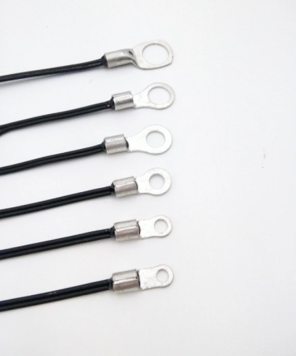
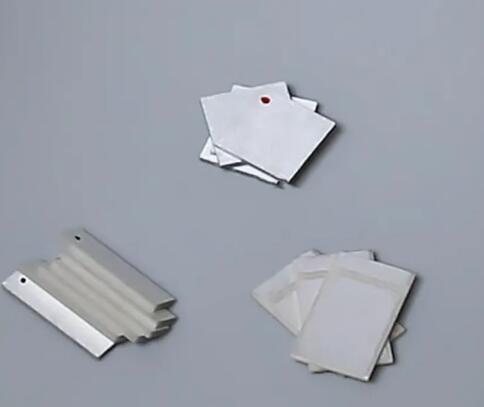
Across the North Sea corridor from Antwerp to Ghent, automated logistics, port IoT equipment, and clean-energy mobility are booming. Integrating our custom NTC temperature sensors, heavy copper layers (up to 4 oz), and aluminum metal-core substrates (MCPCB) guarantees robust thermal conduction away from high-power MOSFETs and charging interfaces, complying with EU automotive standards.
HDI Technical Capability Matrix & Fabrication Thresholds
Direct manufacturing metrics comparing prototype agile runs with mass production capabilities delivered to Western European engineering teams.
| Technical Characteristic | Standard Prototype Capability | Advanced / High-Density Capability | Quality & Validation Standard |
|---|---|---|---|
| Layer Count & Stackup | 4 – 16 Layers (FR-4 Standard) | Up to 32 Layers / Any-Layer HDI (ELIC) | IPC-6012 Class 2 / Class 3 |
| Microvia Laser Drill Size | 0.100 mm (4 mil) CO2 Laser | 0.075 mm (3 mil) UV / CO2 Hybrid | Microsection Cross-Section Analysis |
| Trace Width / Spacing (L/S) | 75 μm / 75 μm (3 / 3 mil) | 50 μm / 50 μm (2 / 2 mil) Modified Semi-Additive (mSAP) | AOI (Automated Optical Inspection) |
| Microvia Plating & Filling | Dimple fill ≤ 15 μm | Copper Filled Via-in-Pad (VIPPO) planarized flush | IPC-4761 Type VII Capped |
| Surface Finishes | ENIG (Electroless Nickel Immersion Gold) | ENEPIG, Immersion Tin, Hard Gold Plating | X-Ray Fluorescence (XRF) Checked |
| Impedance Control Tolerance | ± 10% standard | ± 5% laser precision calibrated | TDR (Time Domain Reflectometry) coupon |
Engineering Review: Get DFM Feedback for Belgian Projects
Avoid expensive re-spins. Upload your RS-274X or ODB++ datasets alongside your BOM for a comprehensive 24-point Design for Manufacturability (DFM) and Design for Assembly (DFA) audit carried out by our senior Shenzhen engineering team.
Why Belgian OEMs Partner with Shenzhen Mivo Electronics
Combining onsite-verified manufacturing muscle with direct, unmediated access to the world's most agile component and electronics manufacturing capital.
Onsite-Verified Factory & Traceability
Shenzhen Mivo Electronics Co., Ltd. has operated continuously since 2016 from Yuanshan Street, Shenzhen. Our premises, staff scale (51–100 specialists), and factory assets are verified through independent, third-party onsite inspections. We hold an 8-year verified export track record with an average international buyer rating of 4.7 out of 5 stars.
Single-Source Turnkey PCBA Integration
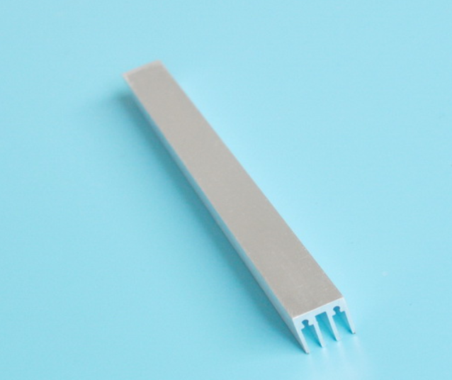
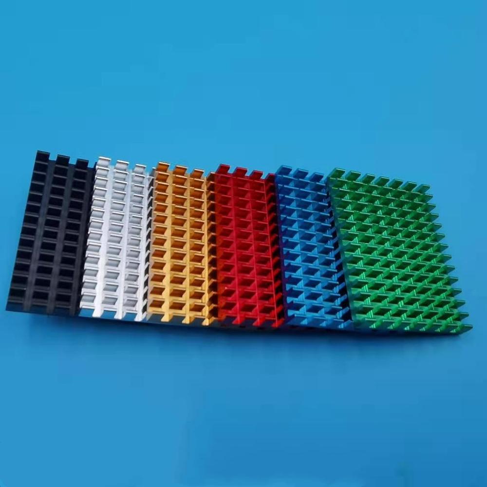
Eliminate the friction of balancing separate board fabricators, component brokers, and surface-mount assemblers. We handle the entire chain: raw PCB fabrication, laser-cut SMT stencils, automated SMT/THT mounting, firmware flashing, and functional testing. Furthermore, we develop custom sensors, high-temperature PT100 probes, and custom aluminum heat sinks.
Low-MOQ Agility & Controlled Lead Times
Innovation cycles should not be held hostage by massive order minimums. We support prototype PCBA batches starting from just 5 pieces, while bare boards start from 100 pieces. For production batches bound for Brussels, Antwerp, or Gent, we coordinate secure DDP/DAP air shipments through Frankfurt, Liège Airport, or Brussels Zaventem within 3 to 7 business days.
Market Dynamics: Emerging PCB Demands in Belgium (2025–2030)
How evolving regulatory frameworks and high-tech sectors in Benelux dictate next-generation circuit board procurement.
EU Circular Economy & WEEE Eco-Design
The European Green Deal and Belgian regional waste legislation demand electronics that withstand prolonged life cycles and simplify recycling. Our halogen-free laminates, lead-free solder pastes (SAC305), and compliance with the RoHS and REACH directives ensure zero regulatory barrier at Antwerp customs, allowing effortless CE certification for end equipment.
Micro-Mobility & Industrial IoT Proliferation
Belgium's dense urban logistics and smart manufacturing corridors require miniaturized computing devices with onboard BLE, 5G, and UWB transceivers. This migration demands thin rigid-flex PCBs and multi-stage sequential buildup HDI boards that fit irregular, hermetically sealed sensor housings without compromising radio-frequency performance.
Thermal Management in E-Mobility
With electric vehicle adoption surging across the Brussels-Capital Region and Flanders, demand for power electronics boards has spiked. Designers must combine high-voltage isolation, thick-copper bus bars, and fast-response thermal sensors (like our 100K B4150 NTC probes) to prevent thermal runaway in high-power lithium battery storage systems.
Procurement FAQ: Sourcing PCBs from China to Belgium
Common questions asked by Belgian procurement officers, hardware engineers, and project leads.
What are the import duties and VAT regulations for PCB/PCBA shipments entering Belgium?
How does Shenzhen Mivo Electronics ensure RoHS and REACH compliance for EU markets?
What specific files are required to begin an HDI PCB and assembly quotation?
What is the typical transit duration from your Shenzhen factory to Brussels or Antwerp?
Can you source specialized or obsolete components for our European designs?
Connect Directly with Our Engineering Team
Partner with an onsite-verified Shenzhen electronics manufacturer trusted by clients across Europe. Inquire now to discuss your stackup specifications, get detailed DFM advice, and download our complete industrial sensor and PCBA product catalog.