Thermal Management
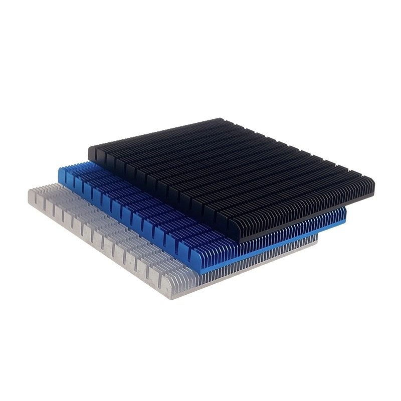
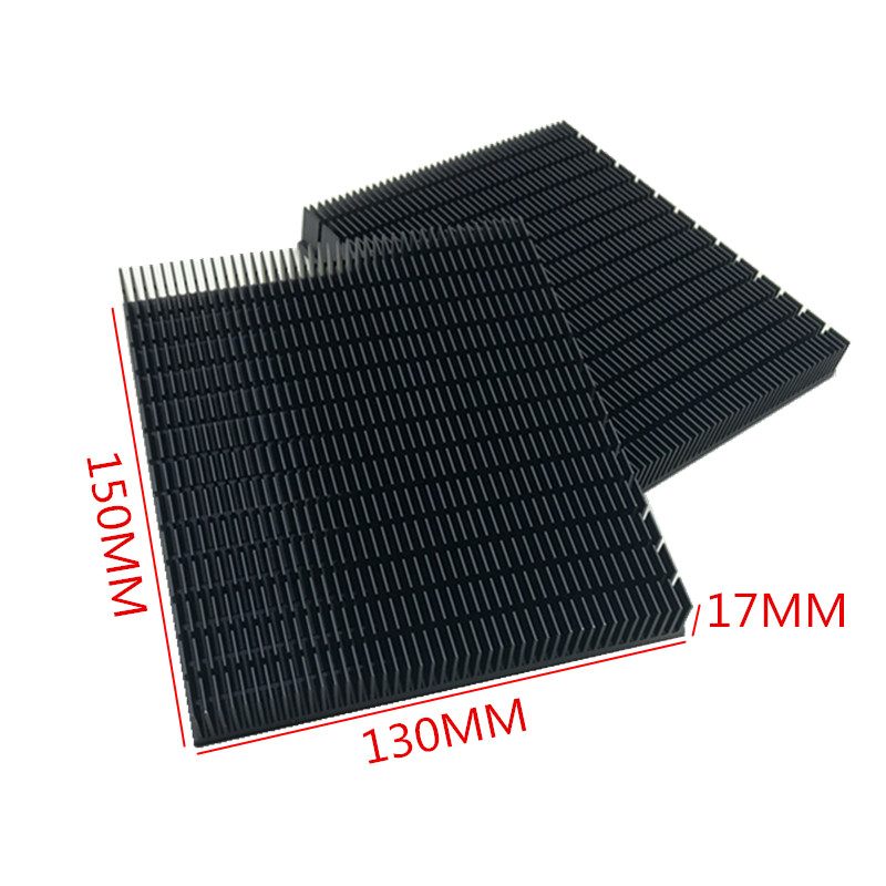
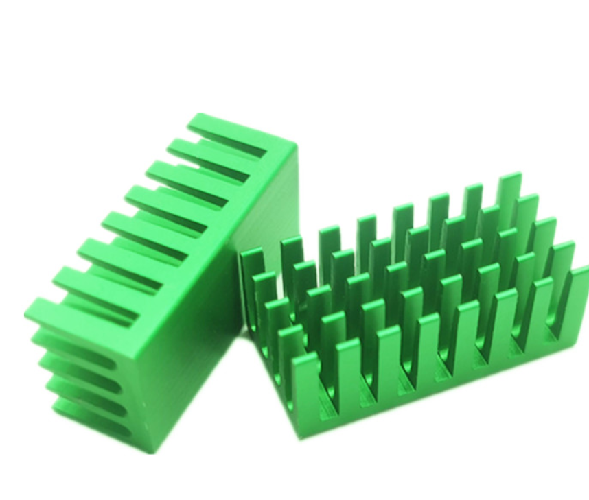
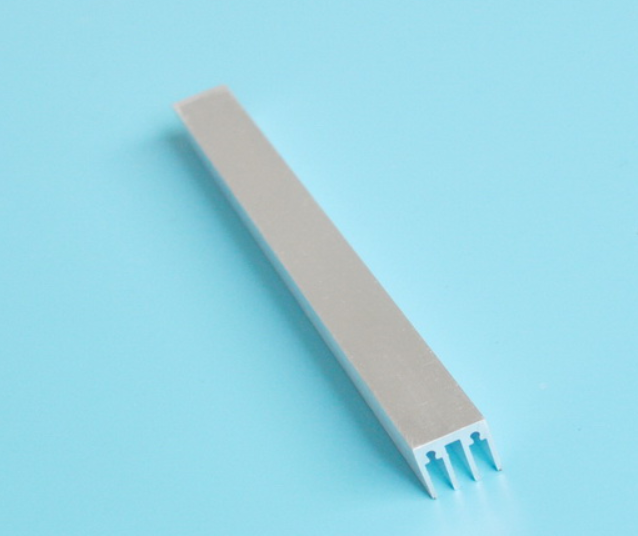
130*100*10mm Aluminum Heatsink Radiator Heat Sink for Electronic RAM Chip PCB LED CPU SSD Cooling With Thermal Conductive Tape
View Details →
Engineered to complement turnkey SMT assembly lines, surface mount solder paste applications, and harsh Atlantic ocean environment deployments.
In high-density surface mount technology (SMT), over 65% of post-reflow soldering defects—including solder bridging, micro-beading, insufficient wetting, voiding, and head-in-pillow (HiP) anomalies—originate directly during the stencil printing phase. As electronic assemblies shrink to accommodate micro-miniaturized wafer-level chip-scale packages (WLCSP), ultra-fine pitch ball grid arrays (BGA pitch ≤ 0.35 mm), and 01005 / 008004 discrete passive components, the mechanical dynamics of solder paste transfer efficiency (PTE) have become the most critical design parameter for industrial product reliability.
At Shenzhen Mivo Electronics Co., Ltd., our custom OEM solder paste stencil engineering strictly adheres to IPC-7525B guidelines while incorporating proprietary laser ablation parameters, chemical electropolishing, and specialized hydrophobic nano-surface finishes. The volume of solder paste transferred from a stencil aperture to the printed circuit board pad is fundamentally dictated by two mechanical constraints: the Aspect Ratio and the Area Ratio.
When engineering stencils for the demanding Atlantic Canadian marine electronics cluster centered in St. John’s, Newfoundland, mechanical tolerances cannot be treated casually. Electronics deployed in harsh subsea exploration, marine environmental telemetry, and naval acoustic systems are routinely conformal-coated, deep-potted in elastomeric polyurethane resins, and exposed to severe cyclic thermal shock (-40°C to +85°C) alongside high ambient hydrostatic pressures. Solder joints possessing hidden voids or unequal intermetallic compound (IMC) thickness inevitably crack during ocean trials. By controlling stencil aperture taper angles between 0.5° and 1.5° and maintaining wall roughness ($Ra$) below 0.35 μm via electropolishing, Mivo Electronics guarantees uniform volumetric paste transfer, near-zero bridging, and robust joint integrity across mission-critical PCBAs.
St. John's, Newfoundland and Labrador stands as Canada’s premier ocean tech gateway. From the innovation corridors around Memorial University of Newfoundland (MUN) and the Marine Institute to offshore operations off the Grand Banks, local hardware engineers demand ruggedized SMT solutions built for extreme Atlantic conditions.
AUV developers in Holyrood and St. John's operate vehicles requiring dense embedded sensor boards, micro-coaxial wiring harnesses, and multichannel acoustic hydrophone modules sealed within titanium pressure hulls.
Oceanographic drifters and offshore weather platforms deployed throughout the Labrador Sea withstand freezing temperatures, wave impacts, and high salt fog corrosion.
Engineering procurement firms supporting Grand Banks offshore supply vessels, subsea wellhead intervention equipment, and coastal clean-energy pilot installations.
Precision stencil manufacturing requires selecting the appropriate foil substrate and post-processing method to match board pitch, assembly volume, and component mix. For engineering laboratories and original equipment manufacturers in St. John’s, balancing tooling costs against line yield is paramount.
| Stencil Technology | Aperture Wall Roughness (Ra) | Minimum Pitch Capability | Paste Release Efficiency | Typical Applications in NL Marine/Tech |
|---|---|---|---|---|
| Standard Laser-Cut SUS304 | 0.65 – 0.85 μm | 0.50 mm (0.020") | 70% – 75% | Standard industrial controllers, low-density power boards, through-hole pin-in-paste. |
| Electropolished Laser-Cut SUS304 | 0.25 – 0.35 μm | 0.40 mm (0.016") | 85% – 90% | Subsea telemetry boards, micro-controller circuits, 0402/0201 passives, BGA assemblies. |
| Electropolished + Nano-Coating | < 0.20 μm | 0.30 mm (0.012") | 95% – 98% | Ultra-dense acoustic sensor nodes, 01005 passives, WLCSP, high-mix R&D prototype lines. |
| Multi-Level Step (Step-Up / Step-Down) | 0.30 – 0.40 μm | Dual-thickness profile | Variable by zone | Mixed assemblies combining heavy current power MOSFETs with 0.4mm pitch FPGAs. |
| Electroformed High-Nickel Foil | < 0.15 μm (atomically smooth) | < 0.30 mm | 98% – 99% | Ultra-high precision aerospace payloads, mission-critical defense electronics, micro-optics. |
For St. John’s engineering teams utilizing automated screen printers (such as DEK, MPM, or manual benchtop tooling at Memorial University incubator hubs), our electropolished stencils equipped with self-cleaning hydrophobic nano-coatings provide dramatically extended print cycles without mid-batch stencil wiping. This preserves solder paste rheology, decreases solvent consumption in remote laboratory environments, and ensures zero defect bridging across fine-pitch BGAs.
Shenzhen Mivo Electronics Co., Ltd. operates an onsite-verified production facility bridging advanced Shenzhen manufacturing efficiencies with rapid air express logistics to Newfoundland and Labrador.
Verified on-premises by Alibaba and third-party inspectors. Active exporter for over 8 years with an authentic 4.7/5 buyer satisfaction index.
Stencils cut concurrently with bare PCB fabrication and turnkey component sourcing, ensuring 100% aperture-to-pad alignment before shipping.
We support Canadian academic, startup, and defense engineering programs with prototype runs starting from just 5 pieces and 24-hour stencil turnaround.
Fast door-to-door courier service (DHL, FedEx, UPS) directly to St. John’s International Airport (YYT) with clear customs documentation and DDP terms.
Precision solder paste stencils are manufactured using state-of-the-art fiber laser cutting machines that operate with beam diameters under 20 μm. Every CAD dataset submitted by St. John’s buyers passes through a rigorous Design for Manufacturability (DFM) check before stainless steel sheets are clamped into laser cutting fixtures.
We analyze paste mask layers (RS-274X, ODB++) against the copper pad layer. Apertures for QFN thermal pads, BGAs, and fine-pitch passives are recalculated for area ratio compliance and home-plate or window-pane geometries.
Using German-engineered fiber laser cutting systems, apertures are cut in high-tensile 304 or 301 stainless steel foil. Micro-cut pulse modulation maintains an aperture taper angle between 0.5° and 1.5° for effortless solder paste release.
Foil undergoes multi-stage electrochemical bath processing to eliminate laser-cut dross, burrs, and micro-ridges. The resulting mirror-smooth aperture walls ($Ra < 0.30$ μm) eliminate paste adhesion friction.
For fine-pitch designs (≤ 0.4 mm BGA or 0201 passives), a specialized organosilicon fluoropolymer coating is applied. This surface treatment repels liquid flux, preventing under-stencil paste bleed during long printing cycles.
Foils are permanently tensioned into high-strength cast aluminum frames (e.g., 29"×29", 23"×23") using multi-ply polyester mesh and solvent-resistant epoxy, maintaining steady tension above 40 N/cm across the entire surface.
Automated optical inspection compares the completed physical stencil against the native Gerber data. Aperture coordinates, missing cutouts, dimensional tolerances, and fiducial markings are validated and certified before dispatch.
Detailed technical, logistical, and commercial answers for electronics engineers, supply chain leads, and contract manufacturers sourcing stencils from Atlantic Canada.
To accelerate file review, minimize turnaround delays, and ensure 100% first-pass printing yields on your SMT line, please include the following technical specifications when requesting a quotation or placing your order:
Send your Gerber files and PCB specifications to our engineering team today. We provide comprehensive DFM feedback, aperture calculation reports, and factory-direct pricing for rapid Canadian delivery.