Precision Electronic Modules & Subcomponents for Geneva OEMs
Direct factory procurement connecting Shenzhen’s agile electronics manufacturing infrastructure with Lake Geneva’s precision instrumentation, research laboratories, and industrial engineering ecosystems.
High-Reliability PCB & PCBA Engineering for Geneva's Advanced Industries
Bridging Swiss micron-level design stringency with high-yield, agile Shenzhen manufacturing pipelines to drastically de-risk prototyping and production cycles.
Overcoming Geneva's Sourcing Paradox: High Spec vs. Velocity
Mission-Critical Hardware Deployment Scenarios
Targeted manufacturing solutions aligned with the technical requirements of Geneva’s dominant industrial, scientific, and environmental sectors.
CERN & Subatomic Research Instrumentation
Geneva's physics sector demands ultra-low-noise acquisition boards capable of withstanding magnetic field exposure and operating reliably in cryogenic detection rigs.
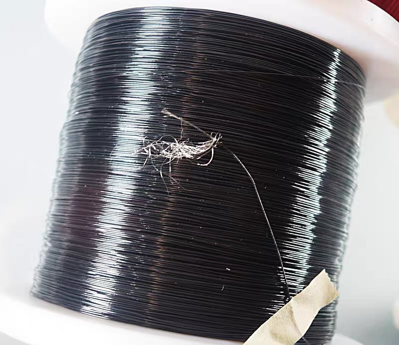
- Sub-0.5mm 36AWG micro-coaxial cable routing
- Low-dielectric Rogers 4350B / Megtron 6 RF stacks
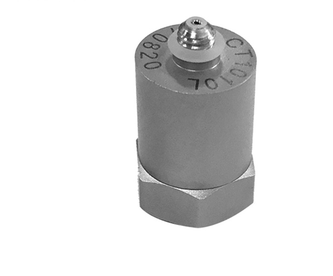
- CT1010L IEPE dynamic vibration acceleration telemetry
- Gold-plated ENIG/ENEPIG pad finishes for wire bonding
Biomedical & Point-of-Care Microfluidics
Supporting diagnostic device developers at Campus Biotech with biocompatible, ultra-dense flexible printed circuits (FPC) and high-precision sensors.
- SHT30/31 calibrated digital thermohygrometric arrays
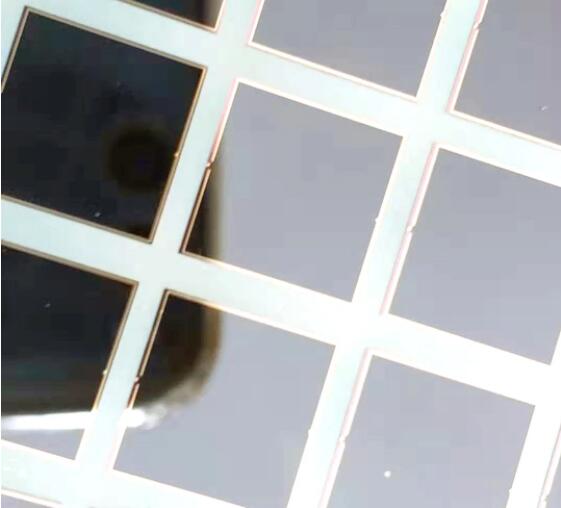
- Bare silicon photodiode integration for spectral assaying
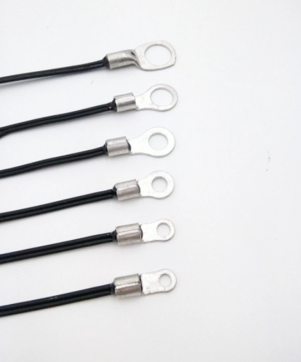
- Miniature PT100 RTD sensor assemblies (5x50mm probes)
- Rigid-flex interconnects fitting tight handheld housings
Luxury Smart Horology & Micro-Mechanics
Geneva's prestigious watchmaking sector increasingly merges traditional Haute Horlogerie finishes with micro-electromechanical systems (MEMS) and smart modules.
- HDI micro-via-in-pad (VIPPO) with 3-mil trace/space
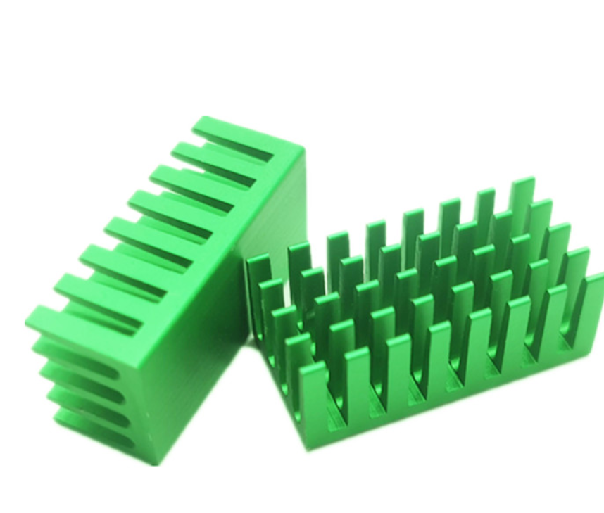
- Sub-millimeter aluminum chip heat spreaders
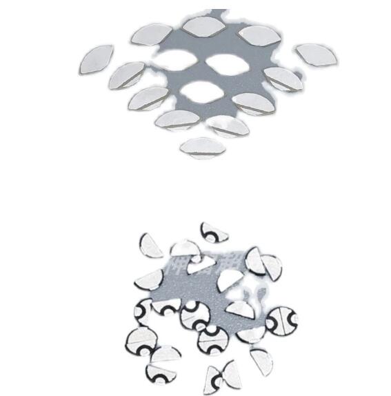
- Piezoelectric PZT multi-frequency acoustic actuators
- Tactile B3SE ultra-low profile micro-switches
Alpine Hydrology & Cleantech Monitoring
Environmental sensors deployed throughout Lake Geneva, the Arve River, and cantonal clean energy facilities monitoring water safety and energy reserves.
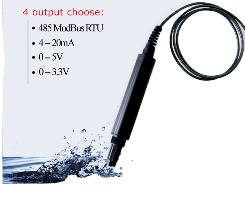
- DOS-600 digital dissolved oxygen RS485 telemetry
- Heavy-copper MCPCBs for power converters
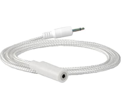
- Water leak detection sensing ropes for archive vaults
- Automotive-grade NTC battery pack temperature probes
Key Technology Trends Shaping Romandy's Hardware Sourcing
A technical evaluation of the shifting architectural requirements across Swiss electronics R&D divisions.
1. Convergence of HDI & Flex Substrates
Micro-mechanisms designed in Geneva increasingly discard traditional wire harnesses in favor of multi-branch flexible printed circuits (FPC) coupled with 4-layer to 10-layer rigid HDI cores. Mivo provides laser-drilled blind and buried vias down to 0.1 mm, utilizing Dupont polyimide films that withstand continuous dynamic flexing without trace fractures.
2. Thermal Stress Mitigation in High-Power Drivers
With electric mobility infrastructure expanding across Swiss cantons and industrial robotics adopting brushless servo architectures, heat dissipation within compact chassis has become paramount. Our metal-core (MCPCB) and direct bonded copper (DBC) fabrication with dielectric thermal conductivities up to 3.0 W/m-K prevent premature silicon degradation.
3. Zero-Defect Component Traceability
European Union and Swiss medical device directives (MDR/IVDR) demand comprehensive part traceability. Mivo implements a rigorous supply chain framework: all active components are purchased directly from original chip manufacturers or authorized tier-one channels, documented via Certificates of Conformance (CoC), and backed by batch-level X-ray inspection.
Substrate & Manufacturing Specification Matrix
| Substrate Technology | Dielectric / Core Material | Min. Trace / Spacing | Surface Finishes Available | Target Swiss Industry Application |
|---|---|---|---|---|
| Standard & HDI Multilayer | FR-4 (Tg 140°C - 180°C), Shengyi S1000-2 | 2.5 mil / 2.5 mil (0.065mm) | ENIG, ENEPIG, Immersion Silver, OSP | Industrial automation controllers, CERN digital backplanes |
| High-Frequency RF & Microwave | Rogers RO4350B, RO4003C, PTFE / Teflon | 3.0 mil / 3.0 mil | Electroless Nickel Immersion Gold (ENIG) | Radar instrumentation, 5G/6G lab equipment, satellite telemetry |
| Flexible Printed Circuit (FPC) | Polyimide (PI) 12.5µm to 50µm, Adhesiveless | 2.0 mil / 2.0 mil | Immersion Gold, Hard Gold fingers | Wearable diagnostics, micro-horology sensor linkages |
| Metal Core PCB (MCPCB) | Aluminum 5052/6061, Copper base (1.0-3.0 W/m-K) | 5.0 mil / 5.0 mil | HASL Lead-Free, White Solder Mask | High-power LED arrays, EV battery BMS, power inverters |
| Rigid-Flex Hybrid | FR-4 + Polyimide with internal air-gap | 3.0 mil / 3.0 mil | ENIG, Selective Gold Plating | Space-constrained avionics, endoscope camera heads |
Direct-from-Source Manufacturing Integrity
Why engineering leads across Switzerland trust Shenzhen Mivo Electronics Co., Ltd. for mission-critical prototype and production orders.
Full Turnkey PCBA Vertical Integration
We eliminate multi-vendor friction. Our Yuanshan Street facility manages bare board production, precision SMT solder paste stencil cutting, BOM procurement, automated pick-and-place, selective wave soldering, conformal coating, and custom firmware flashing under one roof.
Specialized Sensor & Cabling Co-Development
Unlike generic board brokers, Mivo operates dedicated production lines for custom sensor probes and micro-cabling. From RTD PT100 temperature sensors and high-temperature NTC probes to water leakage cables and 36AWG 50Ω coaxial lines, we build complete electro-mechanical sub-assemblies to print.
Verified Supplier Authority & Transparent Metrics
Shenzhen Mivo Electronics has been an onsite-verified supplier on international platforms for over 8 years, holding a 4.7/5 customer rating. Our legal status, manufacturing capacity, and cleanroom facilities undergo independent third-party audit checks, giving overseas buyers complete transactional security.
Frequently Asked Questions by Swiss R&D & Purchasing Teams
Direct answers addressing customs clearances, lead times, regulatory compliance, and quality verification for shipments to Geneva.
How does Mivo manage customs clearance and VAT for delivery into Switzerland (Geneva)?
Shipments to Geneva are typically dispatched via express air couriers (DHL Express, FedEx, or UPS Priority) straight to Geneva Airport (Aéroport de Genève - GVA) or your facility address. All commercial invoices are generated strictly complying with Swiss Federal Customs Administration (FCA) requirements, specifying exact HS codes (e.g., 8534.00 for bare PCBs, 8542.31 for assembled boards).
We support Delivered Duty Paid (DDP) arrangements upon request, where import duties and Swiss Value Added Tax (VAT / MWST / TVA at the standard rate of 8.1%) are handled upfront, ensuring packages clear customs without delay or administrative burden on your receiving dock.
What is Mivo's policy on component substitutions for Swiss medical and precision designs?
Our standard protocol is zero unauthorized substitutions. We purchase strictly according to the specific Manufacturer Part Numbers (MPN) designated in your BOM. If a critical component faces extreme lead-time allocation or factory obsolescence, our component engineering team analyzes footprint-compatible, pin-for-pin cross-references with identical electrical and thermal parameters.
A formal Engineering Change Notice (ECN) accompanied by full manufacturer datasheets is provided to the client. No alternative part is ever placed onto the assembly line without prior written authorization from your engineering team.
What quality testing standards are applied to Geneva-bound PCBA orders?
Every PCBA batch undergoes a multi-tier inspection pipeline conforming to IPC-A-610 Class 2 or Class 3 depending on your end-use specification. Our internal testing arsenal includes:
1. Automated Optical Inspection (AOI): Evaluates solder fillet integrity, component polarity, missing parts, and tombstoning on 100% of boards.
2. X-Ray Inspection (AXI): Verifies void rates and solder ball coalescence underneath QFNs, BGAs, and fine-pitch IC packages.
3. Flying Probe & In-Circuit Testing (ICT): Confirms net connectivity, passive values, and circuit shorts.
4. Functional Circuit Testing (FCT): Custom test jigs and test programs supplied by the client can be integrated directly onto our end-of-line verification stations.
What are the standard delivery lead times from Shenzhen to Geneva?
For quick-turn bare PCB prototypes (2 to 4 layers), standard fabrication takes 3 to 5 business days, with 24-hour rush options available. Turnkey PCBA prototype runs (including component procurement, PCB fabrication, and SMT assembly) typically require 10 to 15 working days depending on parts availability.
Transit via air express from Shenzhen/Hong Kong to Geneva typically takes 3 to 5 business days, ensuring your engineering team receives functional hardware within 3 calendar weeks of design release.
Does Mivo comply with RoHS, REACH, and conflict mineral regulations?
Yes. All circuit board substrates, solder pastes, liquid photoimageable (LPI) solder masks, and procured electronic components fully satisfy EU/Swiss RoHS (Restriction of Hazardous Substances) and REACH (Registration, Evaluation, Authorisation and Restriction of Chemicals) regulations. Declarations of Conformity and Material Safety Data Sheets (MSDS) are provided with production lots upon request.
Accelerate Your Next Hardware Prototype for Geneva
Upload your Gerber RS-274X data, Bill of Materials, and custom sensor drawings. Our bilingual engineering team conducts an initial DFM verification and returns a transparent quote within 24 hours.