Complementary SMT, Sensor & Thermal Components
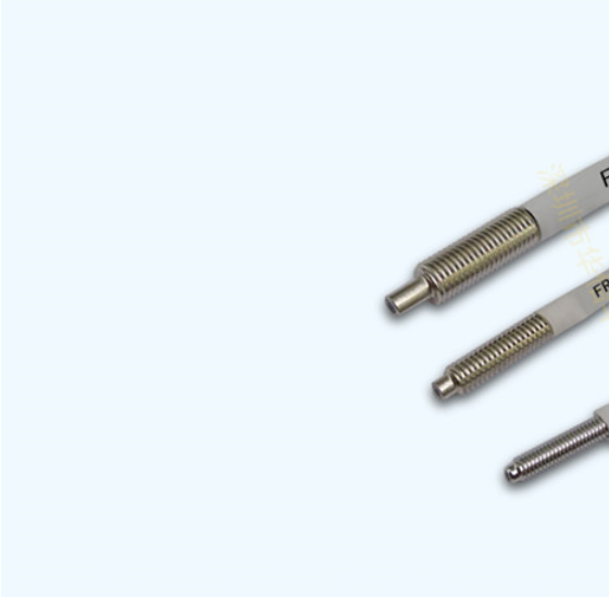
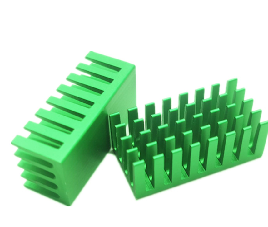
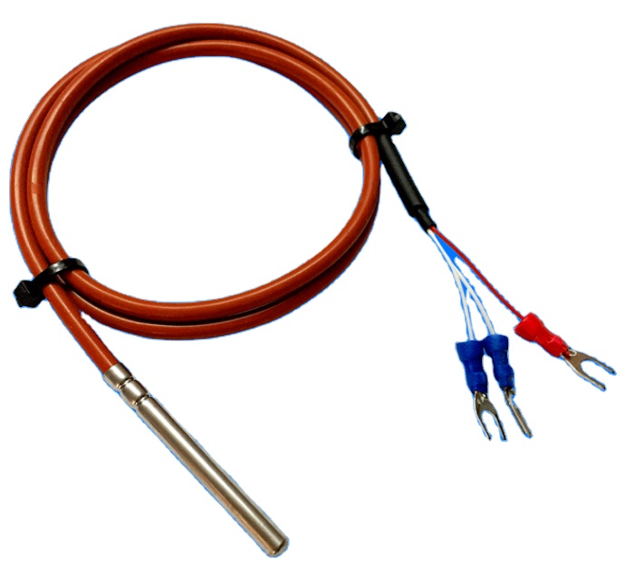
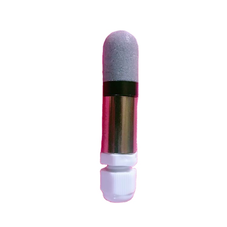
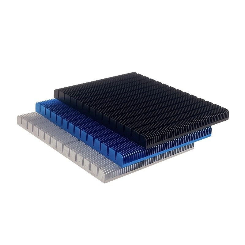
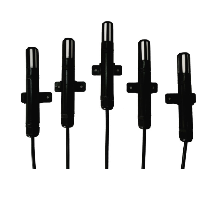
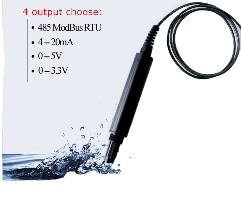
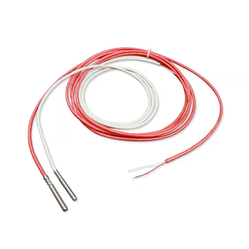
Alongside precision solder stencils, Shenzhen Mivo Electronics exports factory-direct thermal control hardware, optical switches, and platinum RTD probes directly to electronic manufacturing facilities in Paris, Saclay, and broader France.
Aperture Geometry, Aspect Ratios & IPC-7525B Physics
The foundation of zero-defect Surface Mount Technology (SMT) begins at the solder paste printing phase, which accounts for over 64% of all surface mount soldering defects. Our laser-cut stencils are engineered to resolve paste bridging, tombstoning, and insufficient volumetric paste transfer across high-density circuit topologies.
Area Ratio & Aspect Ratio Optimization
Adhering strictly to IPC-7525B standards, our CAD/CAM engineers dynamically calculate both the Area Ratio (Aperture Opening Area divided by Aperture Wall Area, where $AR > 0.66$) and Aspect Ratio (Width divided by Thickness, where $W/T > 1.5$). For ultra-fine pitch components such as 0.3mm pitch CSPs and 01005 passives, we execute custom trapezoidal aperture profiles featuring a 1° to 2° taper, guaranteeing seamless paste detachment with Type 4 and Type 5 solder pastes.
- Strict $AR \ge 0.66$ compliance for ultra-fine micro-BGAs
- Trapezoidal aperture cutting profile ensures 100% paste release
- Custom wall tapering calibrated to paste alloy particle size
Nano-Coating & Surface Metallurgy
Our hydrophobic and oleophobic nano-coatings represent a molecular breakthrough in stencil durability. By modifying the surface energy of SUS304-TA aerospace-grade surgical stainless steel, our nano-technology prevents flux creep and solder bead accumulation on the contact bottom. This reduces automated under-screen wipe cycles from once every 3 boards to once every 20-30 cycles, optimizing takt time on Paris-based automated SMT lines while preserving print-to-print volumetric repeatability.
- Permanent plasma-grafted fluoropolymer molecular barrier
- Surface roughness reduced to Ra < 0.15 µm post-treatment
- Prevents solder bleed underneath stencil during continuous runs
Step-Up & Step-Down Hybrid Topologies
Complex PCBA architectures combining fine-pitch QFNs or 0.4mm BGAs alongside heavy power MOSFETs, D-PAK inductors, or through-hole reflow (THR) pin-in-paste connectors demand varied paste deposition heights. We manufacture specialized multi-level step stencils utilizing micro-milling and micro-welded step-up/step-down techniques. Transition relief pockets are precision-machined with a 1:36 minimum slope ratio, eliminating squeegee blade deformation and ensuring uniform volume across all pad architectures.
- Step thickness delta from 20 µm up to 150 µm variance
- Smooth gradient transitions preventing squeegee skip
- Dual-thickness integration for mixed HDI and power electronics
| Stencil Parameter | Standard Laser-Cut Stencil | Electropolished Nano-Coated Stencil | Multi-Level Step Stencil (Step-Up / Down) |
|---|---|---|---|
| Base Material & Hardness | SUS304 Full Hard Stainless Steel (HV > 380) | SUS304-TA Tension-Annealed Alloy (HV > 420) | Specialized Japanese Ultra-Flat SUS304 Foil |
| Aperture Cut Accuracy | ± 7 µm positioning tolerance | ± 4 µm ultra-high precision fiber laser | ± 5 µm laser cut with CNC milled relief zones |
| Aperture Wall Roughness (Ra) | 0.4 µm – 0.6 µm | < 0.15 µm (Electropolished + Nano-treated) | 0.2 µm on step plane; < 0.18 µm on fine-pitch zone |
| Minimum Component Pitch | 0.5 mm (0201 passive support) | 0.3 mm (01005 passives, 0.35 mm Micro-BGA) | Mixed: 0.3 mm fine-pitch alongside heavy THR connectors |
| Wipe Cycle Frequency | Every 3 to 5 prints | Every 20 to 35 prints (Oleophobic resistance) | Every 10 to 15 prints depending on solder paste alloy |
| Mounting Framework | Cast Aluminum Glued Frame (23"x23", 29"x29") | VectorGuard / Tetra / ZelFlex frameless foils | Custom pneumatic cast aluminum or pre-tensioned frame |
Serving the Paris Hardware Innovation & SMT Corridor
The Greater Paris industrial basin requires rapid iteration cycles, flawless IPC Class 3 quality guarantees, and deep alignment with advanced electronics engineering initiatives across smart mobility, aerospace, defense, and deep-tech hardware.
Paris-Saclay & Deep-Tech R&D Clusters
Dubbed the Silicon Valley of Europe, the Paris-Saclay innovation cluster—spanning Orsay, Palaiseau, and Massy—hosts premier hardware incubators, CNRS scientific institutes, and automotive research hubs. Our expedited rapid-turnaround stencil service provides R&D labs and prototyping centers with customized frameless foils (VectorGuard and ZelFlex compatible) within 72 hours via direct Shenzhen-to-Charles de Gaulle express air cargo, drastically compressing engineering prototype validation times.
Whether assembling radar sensor interfaces, edge AI accelerator computing cards, or micro-fluidic testing devices, our precision apertures maintain the extreme repeatability demanded by high-frequency circuitry.
Aerospace, Defense & Medical IPC-Class 3 EMS
Subcontract manufacturing in the Île-de-France region, extending across Saint-Quentin-en-Yvelines, Évry, and Argenteuil, is anchored by stringent high-reliability contracts. Subcontract EMS factories producing electronics for avionics, defense communications, and Class III medical instruments cannot tolerate solder voids in QFN thermal pads or intermittent open joints.
Our stencils are generated using CAD-driven window-pane algorithms on large thermal pads, reducing solder voiding below 15% (well surpassing standard IPC-A-610 requirements). Stencil foils undergo 100% automated optical inspection (AOI) with aperture dimensional verification reports packaged alongside every dispatch.
Direct Logistics & Engineering Support Across Île-de-France
From fast-track hardware incubators in central Paris (Station F, 13th Arrondissement) to mature EMS production facilities across the wider Parisian manufacturing periphery, our manufacturing process is fully synced with European procurement schedules. Custom Gerber verification (DFM), CAD aperture optimization, and barcode serialization guarantee complete traceability from laser cut to factory squeegee.
Shenzhen Mivo Electronics: Certified Operational Capabilities
Combining localized European market attentiveness with the unyielding production power and speed of Shenzhen's core electronics industrial ecosystem.
Full Turnkey PCBA Ecosystem
Mivo Electronics is more than a stencil workshop: we are an integrated PCB manufacturing, parts sourcing, and turnkey surface-mount assembly provider. We support hardware startups and established OEMs with prototype PCBA runs starting from just 5 pieces, backed by component sourcing with 100% written change approvals for BOM replacements.
Rigorous Engineering DFM Checks
Our CAM department performs complete Design for Manufacturability (DFM) audits prior to laser fabrication. We inspect paste mask layers for solder mask definition, identify prospective bridging on sub-0.4mm pitch ICs, calculate precise volumetric paste requirements for lead-free SAC305 processes, and provide free engineering modification proposals.
Direct Paris Air Logistics & EU Compliance
All stencils are packaged in reinforced ESD wooden/poly cases designed to prevent any warping during high-speed air transit. Utilizing express courier corridors (DHL, FedEx, UPS) directly from Shenzhen Bao'an (SZX) to Paris-Charles de Gaulle (CDG), shipments reach your receiving dock within 48 to 72 hours, fully compliant with EU RoHS 3 and REACH regulations.
Frequently Asked Questions by French SMT Buyers
Transparent technical guidance addressing aperture calculations, printer frame compatibility, delivery transit times to Paris, and customs compliance.
What frame systems do you support for French and European SMT printer lines?
How does your CAM team handle solder bridge mitigation for 0.4mm pitch QFNs and ultra-fine micro-BGAs?
What is the realistic door-to-door transit lead time from your Shenzhen facility to Paris?
Why should Parisian assemblers choose Electropolishing and Nano-Coating for lead-free SAC305 paste?
Are your stencils and electronics parts compliant with EU RoHS 3 and French environmental mandates?
What specific files do you require to begin production of an SMT stencil?
Optimize Your SMT Solder Printing Performance Today
Consult with our senior CAM engineers, discuss customized aperture reductions, or request an immediate quote for custom laser-cut, nano-coated, or multi-level step stencils delivered directly to your facility in Paris or across Île-de-France.
Send an Inquiry