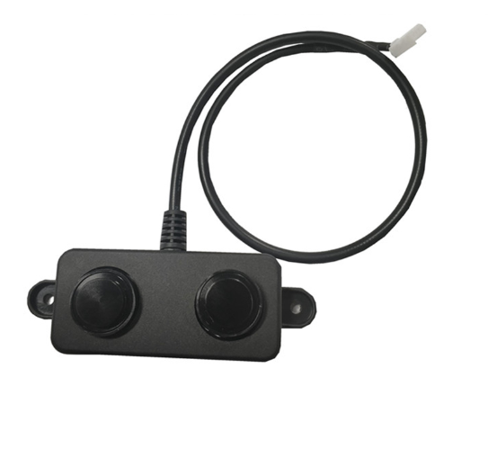
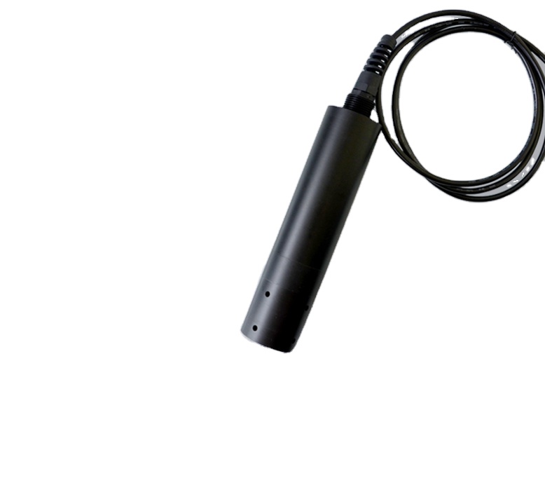
Ultrasonic Sensor
Directly integrated into surface-mount PCB assembly runs, automated lines, and industrial thermal management assemblies across Sheffield and Rotherham research facilities.
In high-reliability electronics manufacturing, print quality dictates overall SMT (Surface Mount Technology) assembly line yields. Empirical studies consistently demonstrate that between 60% and 75% of all soldering anomalies—including bridging, solder balling, insufficient volume, voiding, and head-in-pillow (HiP) defects—originate directly during the solder paste deposition process. As board designs in South Yorkshire's advanced manufacturing cluster trend toward extreme miniaturization, combining ultra-fine pitch ball grid arrays (micro-BGAs at 0.3mm pitch) with power-handling QFNs and 01005 passive elements, the precision of the SMT stencil has become the primary determinator of baseline yield.
Sheffield, internationally renowned as a historical powerhouse of metallurgy and precision tool engineering, has transformed into a high-technology corridor anchored by the Advanced Manufacturing Research Centre (AMRC) and the Olympic Legacy Park innovation zones. Electronic design firms and contract electronics manufacturers (CEMs) operating within Sheffield, Rotherham, and the wider Don Valley require high-capability SMT solder paste stencils that comply with stringent IPC-7525B engineering requirements. Selecting the correct stencil manufacturing factory involves analyzing laser beam spot optics, foil metallurgy (SUS304-FG vs. fine-grain SUS430), post-cutting electrochemical polishing, and functional surface treatments like plasma nano-coatings.
Procurement teams serving Sheffield's industrial electronics sector must evaluate the metallurgical tradeoffs between different stencil production techniques. While chemically etched stencils have essentially become obsolete for fine-pitch SMT, precision fiber-laser machining and additive electroforming define the modern manufacturing baseline.
| Stencil Technology | Aperture Wall Quality | Positional Accuracy | Minimum Component Pitch | Ideal Application Sector |
|---|---|---|---|---|
| Standard Laser-Cut (SUS304) | Striated laser taper; mechanically deburred | ±9μm | 0.50 mm (QFP, SOIC, 0402) | Industrial automation prototypes, basic power supplies |
| Fine-Grain Laser + Electropolished | Smooth mirror finish; Ra < 0.2μm | ±4μm | 0.40 mm (0201, QFN, DFN) | Sheffield rail traction telemetry, medical sensory nodes |
| Direct-Laser + Hydrophobic Nano-Coated | Oleophobic fluoropolymer layer prevents paste creep | ±2μm | 0.30 mm (01005, 0.3mm BGA, WLCSP) | AMRC aerospace avionics, compact IoT wearable devices |
| Additive Electroformed (Nickel) | Molecularly uniform, zero taper, trapezoidal walls | ±1.5μm | < 0.30 mm ultra-fine pitch | Ultra-precision defence optics, specialized silicon packaging |
| Step-Down / Step-Up Multi-Level | Dual-thickness chemically milled or micro-machined pocket | ±5μm | Mixed: 0.3mm mixed with massive connectors | High-power automotive EV battery management systems (BMS) |
Our engineering research team evaluated hundreds of fabrication facilities worldwide to identify the top 10 stencil suppliers capable of serving Sheffield's demanding contract manufacturing, university research, and high-reliability aerospace environments. Factories were evaluated on technical capability (aperture positional tolerance, fine-grain steel foil availability, nano-coating chemistry), turn-around speed, DFM support, and international supply reliability.
An onsite-verified electronics manufacturer established in 2016, Mivo Electronics operates comprehensive SMT stencil laser cutting alongside turnkey PCB fabrication, surface-mount assembly, custom sensor builds, and thermal components. Specializing in prototype runs from 5 pieces to volume production with direct Gerber review.
The benchmark for industrial automated screen printing. ASM's DEK stencil division provides VectorGuard framed foil systems, electroformed stencils, and high-spec nano-coatings widely utilized in high-volume UK automotive assembly plants.
One of the UK's longest-standing dedicated laser stencil toolmakers. Provides rapid same-day and next-day stencil turnaround across England with extensive multi-level stepped stencil milling capabilities.
Pioneers in high-density electroformed stencils and specialized thick-film print screens. Ideal for Sheffield medical instrument makers fabricating miniaturized sub-modules with microscopic deposit tolerances.
Specializes in precision micro-chemical etching and high-end laser machining of metal foils. Provides advanced multi-level 3D step stencils used extensively in power electronics and RF transceiver modules.
Operating one of the UK’s most advanced microelectronics cleanrooms, CIL delivers precision laser-cut foils specifically optimized for wide-bandgap SiC and GaN semiconductor substrate assembly.
Supplies high-grade laser stencils matched precisely to Alpha, Indium, and Kester solder chemistry. Offers robust technical consultation regarding flux vehicle activation and release dynamics.
Global authority on laser stencil cutting technology. Stencils produced on LPKF StencilLaser G 6080 systems offer industry-leading aperture corner radius execution down to 5μm, minimizing paste entrapment.
European specialist in hybrid screen-stencil assemblies and thick-film sensor print heads. Extensively specified in solar panel cell production and precision automotive hybrid thick-film electronics.
Renowned for low-cost, fast-turnaround frameless prototype stainless steel foils. Widely used by Sheffield Hallam University, University of Sheffield engineering labs, and quick-turn hardware incubators.
Sheffield's manufacturing profile is uniquely driven by high-integrity materials, energy transition projects, medical devices, and advanced aerospace programs. SMT stencils destined for South Yorkshire facilities operate in specialized production settings requiring custom aperture modifications:
Sheffield's Olympic Legacy Park medical corridor fabricates endoscopic diagnostic tools, intelligent surgical probes, and sterilization-proof sensory nodes. These PCBA designs demand electroformed or nano-coated stencils for 0201 passives and high-density flex-rigid circuits.
Anchored by the world's largest electrolyzer gigafactory in Sheffield, clean energy telemetry demands heavy-copper PCBs (3oz to 6oz). SMT stencils require multi-level step-down milling to handle heavy power busbars simultaneously with sensitive 0.4mm microcontrollers.
In collaboration with the University of Sheffield AMRC, aerospace structural telemetry systems deploy sensor nodes directly into composite airframes. Stencils must feature zero-dross aperture edges and precise home-plate geometry to eliminate solder voids under thermal vibration.
South Yorkshire’s rolling stock supply network requires high-durability IGBT driver boards. Stencils for these boards require specialized cross-hatching apertures on massive thermal pads to avoid solder paste spatter during vacuum-assisted reflow soldering.
Building on historical mining engineering strengths, local geotechnical companies construct rugged downhole sensors. Electronics feature thick substrates and high-melting-point solder pastes, requiring sturdy 150μm to 180μm laser-cut stainless foils.
Industrial robotics startups at the AMP utilize embedded controller boards housing multi-core microprocessors. These tight layouts utilize 100μm foils treated with permanent fluoropolymer nano-coatings to ensure zero solder bridges between adjacent high-speed signal pins.
Historically, UK manufacturing facilities sourced all tooling exclusively from domestic machine shops. Over the past five years, however, supply chain shocks and margin pressures have caused Sheffield purchasing directors to adopt a hybrid procurement model. For urgent 12-hour benchtop fixes, local UK laser shops remain valuable; however, for prototype-to-volume NPI (New Product Introduction), turnkey Chinese partners like Shenzhen Mivo Electronics provide unmatched commercial and technical advantages.
By producing the bare multilayer PCB, sourcing original active ICs through Shenzhen's authorized distribution hubs, cutting the matched stainless steel SMT stencil, and handling pick-and-place assembly under one unified roof, engineering discrepancies are resolved prior to tooling creation. A single Gerber package uploaded to Mivo avoids the common friction where the stencil vendor blames the PCB fabricator for solder mask expansion mismatches.
Shenzhen Mivo Electronics Co., Ltd. is an onsite-verified electronics manufacturer located in Shenzhen, Guangdong, China. We bridge the gap between high-precision Chinese supply chain agility and Western engineering reliability standards. We do not simply cut stencils; we build complete turnkey electronic systems—from bare rigid, multilayer, aluminum-core, and flexible circuit boards, to precision SMT stencils, complex cable harnesses, membrane switches, and industrial sensor modules.
With an onsite-checked facility, an average customer satisfaction score of 4.7 out of 5 stars over 8 years on Alibaba.com, and prototype minimum orders starting from just 5 pieces, we ensure complete supply transparency and verified BOM component authentication for overseas engineering teams.
Contact UsClear answers to the most common engineering, logistics, and DFM inquiries encountered by UK electronics engineers.
We require the solder paste layer file (commonly designated as .GTP for top paste or .GBP for bottom paste) in RS-274X or ODB++ format. Including the board outline (mechanical layer) and solder mask files is recommended so our DFM engineers can cross-verify fiducial placements and verify aperture reductions for high-density components.
Nano-coating is strongly recommended whenever your design contains components with a pitch ≤ 0.5mm, 0201/01005 passive chips, or QFN/BGA packages where the IPC Area Ratio drops below 0.66. The hydrophobic and oleophobic plasma coating prevents solder paste from clinging to the interior aperture walls, increasing paste transfer efficiency up to 98% and reducing underside wiping frequency.
Yes. We supply framed stencils in all international standard cast-aluminum frame dimensions (such as 23×23 inches, 29×29 inches, 584×584mm, and 736×736mm) fully pneumatic-glued with solvent-resistant polyester/stainless mesh. We also supply frameless foils pre-punched for ZelFlex, VectorGuard, and Alpha Tetra quick-clamping systems commonly used across UK manufacturing sites.
Our engineering DFM team performs automatic aperture reduction calculations based on component pin geometries. For central exposed ground pads (thermal pads on QFNs and power ICs), we automatically replace monolithic cutouts with window-pane or cross-hatched arrays (typically 60% to 70% paste area coverage) to eliminate solder spatter and catastrophic component tilting.
Once CAD files are approved, laser cutting and electro-polishing are completed in 12 to 24 hours. Express air shipping via DHL Express, FedEx Priority, or UPS directly to Sheffield, Rotherham, or Manchester addresses takes approximately 3 to 5 business days, complete with tracking and clear UK customs customs clearance documentation.
We cater directly to prototyping and low-volume production. Laser-cut stencils have an MOQ of just 1 piece. Turnkey prototype PCBA projects start from 5 pieces. Bare PCB manufacturing batches typically begin at 100 pieces, while specialized sensor modules start from 10 pieces, and catalogue components range from 100 to 2,000 units depending on packaging.
Send us your Gerber files, BOM, or mechanical drawings today. Mivo Electronics' technical engineering team will deliver a comprehensive DFM audit, stencil aperture evaluation, and factory-direct quotation within 24 hours.